
Datasheet


PIC16(L)F1512/3
DS41624B-page 150 Preliminary 2012 Microchip Technology Inc.
16.6.8 GUARD RING OUTPUTS
Guard ring drive is a pair of digital outputs from the
ADC module. This function is enabled by the GRDAOE
and GRDBOE bits of the AADGRD register. Polarity of
the output is controlled by the GRDPOL bit.
The guard ring outputs of the ADC are active at all
times. The outputs are initialized at the start of the pre-
charge stage to match the polarity of the GRDPOL bit.
The guard output signal changes polarity at the start of
the acquisition stage. The value stored by the
GRDPOL bit does not change.
When in Double Sampling mode, the guard ring output
does not initialize on the second conversion. It toggles
polarity at the start of the first acquisition stage and
again for the second acquisition, back to the original
state. For more information on the timing of the guard
ring output refer to Figure 16-8 and Figure 16-10.
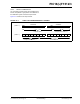
A typical guard ring circuit is displayed in Figure 16-11.
C
GUARD represents the capacitance of the guard ring
trace placed on a PCB board. The user selects values
for R
A and RB that cause the voltage profile of CGUARD
to match the selected channel during acquisition.
FIGURE 16-11: USER GUARD RING
CIRCUIT
16.6.9 ADDITIONAL SAMPLE AND HOLD
CAPACITOR
Additional capacitance can be added in parallel with the
sample and hold capacitor (C
HOLD) by setting the
ADDCAP<2:0> bits of AADCAP register. This bit
connects additional capacitance to the ADC conversion
bus, increasing the effective internal capacitance of the
A/D module and analog bus. The additional capacitance
does not affect analog performance of the ADC because
it is not connected during conversion. See Figure 16-12.
CGUARD
RA
RB
ADGRDA
ADGRDB