
Datasheet


PIC16(L)F1512/3
DS41624B-page 147 Preliminary 2012 Microchip Technology Inc.
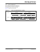
FIGURE 16-8: DOUBLE SAMPLE CONVERSION SEQUENCE (ADDSEN = 1, ADIPEN = 1, GUARD-RING, GRDPOL = 1)
9th 8th 7th
6th
5th
4th 3rd 2nd 1st
Second result
1-127 T
INST
TAD
Conversion Clock
AADRESxL/H<9:0>
Note 1: When conversion clock is ADCRC, Pre-Charge and Acquisition Timers are clocked by ADCRC.
10’h000
written to
9th 8th
7th 6th
5th
4th 3rd
2nd
1st10’h000
First result ready
Pre-Charge
AADPRE[6:0]
Acquisition
AADACQ[6:0]
Pre-Charge
AADPRE[6:0]
Acquisition
AADACQ[6:0]
AADRES1L/H
First result
written to
AADRES0L/H
ANx
Digital
‘1’ Out
Digital
‘0’ Out
GO/DONE
1-127 T
INST
1-127 T
INST
1-127 T
INST
TPRE
TACQ
TCONV
(1)
(1)
(1)
(1)
2
INST
TPRE
TACQ
TCONV
ADSTAT[2:0]
3’b001
3’b010
3’b011
3’b101 3’b110
3’b111
3’b000
Analog
Input
TRISx<x> Control
Analog
Input
TRISx<x> Control
ADGRDA
ADGRDB
Guard A and B
Initialized
Guard A and B
Initialized
(ADEPPOL = 1)
CHOLD
(ADIPPOL = 0)
Shorted to
V
REFL
Hold during conversion
Shorted to
V
REFH
Hold during conversion
Charge
sharing
Charge
sharing