
Datasheet


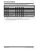


Table Of Contents
- 20-Pin Flash, 8-Bit Microcontrollers with XLP Technology
- PIC12(L)F1501/PIC16(L)F150X Family Types
- Pin Diagrams
- Pin Allocation Table
- TABLE 1: 20-Pin Allocation Table (PIC16(L)F1508/9)
- Table of Contents
- 1.0 Device Overview
- 2.0 Enhanced Mid-Range CPU
- 3.0 Memory Organization
- TABLE 3-1: Device Sizes and Addresses
- FIGURE 3-1: Program Memory Map And Stack For PIC16(L)F1508
- FIGURE 3-2: Program Memory Map And Stack For PIC16(L)F1509
- TABLE 3-2: Core Registers
- FIGURE 3-3: Banked Memory Partitioning
- TABLE 3-3: PIC16(L)F1509 Memory Map, Bank 1-7
- TABLE 3-4: PIC16(L)F1508 Memory Map, Bank 1-7
- TABLE 3-5: PIC16(L)F1508/9 Memory Map, Bank 8-23
- 3.1 Program Memory Organization
- FIGURE 3-11: Linear Data Memory Map
- TABLE 3-6: PIC16(L)F1508/9 Memory Map, Bank 24-31
- TABLE 3-7: PIC16(L)F1508/9 Memory Map, Bank 30-31
- TABLE 3-8: Core Function Registers Summary
- TABLE 3-9: Special Function Register Summary
- FIGURE 3-4: Loading of PC in Different Situations
- FIGURE 3-5: Accessing the Stack Example 1
- FIGURE 3-6: Accessing the Stack Example 2
- FIGURE 3-7: Accessing the Stack Example 3
- FIGURE 3-8: Accessing the Stack Example 4
- FIGURE 3-9: Indirect Addressing
- FIGURE 3-10: Traditional Data Memory Map
- FIGURE 3-12: Program Flash Memory Map
- 4.0 Device Configuration
- 4.1 Configuration Words
- 4.2 Register Definitions: Configuration Words
- Register 4-1: CONFIG1: Configuration Word 1
- Register 4-2: CONFIG2: Configuration Word 2
- 4.3 Code Protection
- 4.4 Write Protection
- 4.5 User ID
- 4.6 Device ID and Revision ID
- 4.7 Register Definitions: Device ID
- Register 4-3: DEVID: Device ID Register
- 5.0 Oscillator Module (With Fail-Safe Clock Monitor)
- FIGURE 5-1: Simplified PIC® MCU Clock Source Block Diagram
- FIGURE 5-2: External Clock (EC) Mode Operation
- FIGURE 5-3: Quartz Crystal Operation (LP, XT or HS Mode)
- FIGURE 5-4: Ceramic Resonator Operation (XT or HS Mode)
- FIGURE 5-5: Quartz Crystal Operation (Secondary Oscillator)
- FIGURE 5-6: External RC Modes
- TABLE 5-1: Peripheral Clock Sources
- FIGURE 5-7: Internal Oscillator Switch Timing
- TABLE 5-2: OSTS Bit Definition
- TABLE 5-3: Oscillator Switching Delays
- FIGURE 5-8: Two-Speed Start-up
- FIGURE 5-9: FSCM Block Diagram
- FIGURE 5-10: FSCM Timing Diagram
- TABLE 5-4: Summary of Registers Associated with Clock Sources
- 5.1 Overview
- TABLE 5-5: Summary of Configuration Word with Clock Sources
- 6.0 Resets
- FIGURE 6-1: Simplified Block Diagram of On-Chip Reset Circuit
- TABLE 6-1: BOR Operating Modes
- FIGURE 6-2: Brown-out Situations
- TABLE 6-2: MCLR Configuration
- FIGURE 6-3: Reset Start-up Sequence
- TABLE 6-3: Reset Status Bits and Their Significance
- TABLE 6-4: Reset Condition for Special Registers
- TABLE 6-5: Summary of Registers Associated with Resets
- TABLE 6-6: Summary of Configuration Word with Resets
- 7.0 Interrupts
- FIGURE 7-1: Interrupt Logic
- FIGURE 7-2: Interrupt Latency
- FIGURE 7-3: INT Pin Interrupt Timing
- 7.3 Interrupts During Sleep
- 7.4 INT Pin
- 7.5 Automatic Context Saving
- 7.6 Register Definitions: Interrupt Control
- Register 7-1: INTCON: Interrupt Control Register
- Register 7-2: PIE1: Peripheral Interrupt Enable Register 1
- Register 7-3: PIE2: Peripheral Interrupt Enable Register 2
- Register 7-4: PIE3: Peripheral Interrupt Enable Register 3
- Register 7-5: PIR1: Peripheral Interrupt Request Register 1
- Register 7-6: PIR2: Peripheral Interrupt Request Register 2
- Register 7-7: PIR3: Peripheral Interrupt Request Register 3
- TABLE 7-1: Summary of Registers Associated with Interrupts
- 8.0 Power-Down Mode (Sleep)
- 9.0 Watchdog Timer (WDT)
- 10.0 Flash Program Memory Control
- TABLE 10-1: Flash Memory Organization by Device
- FIGURE 10-1: Flash Program Memory Read Flowchart
- FIGURE 10-2: Flash Program Memory Read Cycle Execution
- FIGURE 10-3: Flash Program Memory Unlock Sequence Flowchart
- FIGURE 10-4: Flash Program Memory Erase Flowchart
- FIGURE 10-5: Block Writes to Flash Program Memory with 32 Write latches
- FIGURE 10-6: Flash Program Memory Write Flowchart
- FIGURE 10-7: Flash Program Memory Modify Flowchart
- TABLE 10-2: User ID, Device ID and Configuration Word Access (CFGS = 1)
- 10.1 PMADRL and PMADRH Registers
- 10.2 Flash Program Memory Overview
- FIGURE 10-8: Flash Program Memory Verify Flowchart
- 10.6 Register Definitions: Flash Program Memory Control
- Register 10-1: PMDATL: Program Memory Data Low Byte Register
- Register 10-2: PMDATH: Program Memory Data High Byte Register
- Register 10-3: PMADRL: Program Memory Address Low Byte Register
- Register 10-4: PMADRH: Program Memory Address High Byte Register
- Register 10-5: PMCON1: Program Memory Control 1 Register
- Register 10-6: PMCON2: Program Memory Control 2 Register
- TABLE 10-3: Summary of Registers Associated with Flash Program Memory
- TABLE 10-4: Summary of Configuration Word with Flash Program Memory
- 11.0 I/O Ports
- TABLE 11-1: Port Availability Per Device
- FIGURE 11-1: Generic I/O Port Operation
- TABLE 11-2: PORTA Output Priority
- TABLE 11-3: Summary of Registers Associated with PORTA
- TABLE 11-4: Summary of Configuration Word with PORTA
- TABLE 11-5: PORTB Output Priority
- TABLE 11-6: Summary of Registers Associated with PORTB
- TABLE 11-7: Summary of Configuration Word with PORTB
- TABLE 11-8: PORTC Output Priority
- TABLE 11-9: Summary of Registers Associated with PORTC
- 12.0 Interrupt-On-Change
- FIGURE 12-1: Interrupt-On-Change Block Diagram (PORTA Example)
- 12.6 Register Definitions: Interrupt-on-Change Control
- Register 12-1: IOCAP: Interrupt-on-Change PORTA Positive Edge Register
- Register 12-2: IOCAN: Interrupt-on-Change PORTA Negative Edge Register
- Register 12-3: IOCAF: Interrupt-on-Change PORTA Flag Register
- Register 12-4: IOCBP: Interrupt-on-Change PORTB Positive Edge Register
- Register 12-5: IOCBN: Interrupt-on-Change PORTB Negative Edge Register
- Register 12-6: IOCBF: Interrupt-on-Change PORTB Flag Register
- TABLE 12-1: Summary of Registers Associated with Interrupt-on-Change
- 12.1 Enabling the Module
- 12.2 Individual Pin Configuration
- 12.3 Interrupt Flags
- 12.4 Clearing Interrupt Flags
- EXAMPLE 12-1: Clearing Interrupt Flags (PORTA Example)
- 12.5 Operation in Sleep
- FIGURE 12-1: Interrupt-On-Change Block Diagram (PORTA Example)
- 13.0 Fixed Voltage Reference (FVR)
- 14.0 Temperature Indicator Module
- 15.0 Analog-to-Digital Converter (ADC) Module
- FIGURE 15-1: ADC Block Diagram
- TABLE 15-1: ADC Clock Period (Tad) Vs. Device Operating Frequencies
- FIGURE 15-2: Analog-to-Digital Conversion Tad Cycles
- FIGURE 15-3: 10-Bit ADC Conversion Result Format
- TABLE 15-2: Auto-Conversion Sources
- EXAMPLE 15-1: ADC Conversion
- 15.3 Register Definitions: ADC Control
- Register 15-1: ADCON0: ADC Control Register 0
- Register 15-2: ADCON1: ADC Control Register 1
- Register 15-3: ADCON2: ADC Control Register 2
- Register 15-4: ADRESH: ADC Result Register High (ADRESH) ADFM = 0
- Register 15-5: ADRESL: ADC Result Register Low (ADRESL) ADFM = 0
- Register 15-6: ADRESH: ADC Result Register High (ADRESH) ADFM = 1
- Register 15-7: ADRESL: ADC Result Register Low (ADRESL) ADFM = 1
- 15.4 ADC Acquisition Requirements
- EQUATION 15-1: Acquisition Time Example
- FIGURE 15-4: Analog Input Model
- FIGURE 15-5: ADC Transfer Function
- TABLE 15-3: Summary of Registers Associated with ADC
- 16.0 5-Bit Digital-to-Analog Converter (DAC) Module
- FIGURE 16-1: Digital-to-Analog Converter Block Diagram
- 16.1 Output Voltage Selection
- 16.2 Ratiometric Output Level
- 16.3 DAC Voltage Reference Output
- 16.4 Operation During Sleep
- 16.5 Effects of a Reset
- EQUATION 16-1: DAC Output Voltage
- 16.6 Register Definitions: DAC Control
- Register 16-1: DACxCON0: Voltage Reference Control Register 0
- Register 16-2: DACxCON1: Voltage Reference Control Register 1
- TABLE 16-1: Summary of Registers Associated with the DAC Module
- FIGURE 16-1: Digital-to-Analog Converter Block Diagram
- 17.0 Comparator Module
- TABLE 17-1: Available Comparators
- FIGURE 17-1: Comparator Module Simplified Block Diagram
- FIGURE 17-2: Single Comparator
- TABLE 17-2: Comparator Output State vs. Input Conditions
- FIGURE 17-3: Analog Input Model
- FIGURE 17-4: Analog Input Model
- 17.4 Comparator Hysteresis
- 17.5 Timer1 Gate Operation
- 17.6 Comparator Interrupt
- 17.7 Comparator Response Time
- 17.8 Register Definitions: Comparator Control
- Register 17-1: CMxCON0: Comparator Cx Control Register 0
- Register 17-2: CMxCON1: Comparator Cx Control Register 1
- Register 17-3: CMOUT: Comparator Output Register
- TABLE 17-3: Summary of Registers Associated with Comparator Module
- 17.1 Comparator Overview
- 18.0 Timer0 Module
- 19.0 Timer1 Module with Gate Control
- FIGURE 19-1: Timer1 Block Diagram
- TABLE 19-1: Timer1 Enable Selections
- TABLE 19-2: Clock Source Selections
- TABLE 19-3: Timer1 Gate Enable Selections
- TABLE 19-4: Timer1 Gate Sources
- FIGURE 19-2: Timer1 Incrementing Edge
- FIGURE 19-3: Timer1 Gate Enable Mode
- FIGURE 19-4: Timer1 Gate Toggle Mode
- FIGURE 19-5: Timer1 Gate Single-Pulse Mode
- FIGURE 19-6: Timer1 Gate Single-Pulse and Toggle Combined Mode
- TABLE 19-5: Summary of Registers Associated with Timer1
- 20.0 Timer2 Module
- 21.0 Master Synchronous Serial Port (MSSP) Module
- FIGURE 21-1: MSSP Block Diagram (SPI mode)
- FIGURE 21-2: MSSPx Block Diagram (I2C™ Master mode)
- FIGURE 21-3: MSSP Block Diagram (I2C™ Slave mode)
- FIGURE 21-4: SPI Master and Multiple Slave Connection
- FIGURE 21-5: SPI Master/Slave Connection
- FIGURE 21-6: SPI Mode Waveform (Master Mode)
- FIGURE 21-7: SPI Daisy-Chain Connection
- FIGURE 21-8: Slave Select Synchronous Waveform
- FIGURE 21-9: SPI Mode Waveform (Slave Mode With CKE = 0)
- FIGURE 21-10: SPI Mode Waveform (SLAve Mode With CKE = 1)
- 21.1 MSSP Module Overview
- TABLE 21-1: Summary of Registers Associated with SPI Operation
- FIGURE 21-11: I2C Master/ Slave Connection
- TABLE 21-2: I2C Bus terms
- FIGURE 21-12: I2C Start and Stop Conditions
- FIGURE 21-13: I2C Restart Condition
- FIGURE 21-14: I2C Slave, 7-bit Address, Reception (SEN = 0, AHEN = 0, DHEN = 0)
- FIGURE 21-15: I2C Slave, 7-bit Address, Reception (SEN = 1, AHEN = 0, DHEN = 0)
- FIGURE 21-16: I2C Slave, 7-bit Address, Reception (SEN = 0, AHEN = 1, DHEN = 1)
- FIGURE 21-17: I2C Slave, 7-bit Address, Reception (SEN = 1, AHEN = 1, DHEN = 1)
- FIGURE 21-18: I2C Slave, 7-bit Address, Transmission (AHEN = 0)
- FIGURE 21-19: I2C Slave, 7-bit Address, Transmission (AHEN = 1)
- FIGURE 21-20: I2C Slave, 10-bit Address, Reception (SEN = 1, AHEN = 0, DHEN = 0)
- FIGURE 21-21: I2C Slave, 10-bit Address, Reception (SEN = 0, AHEN = 1, DHEN = 0)
- FIGURE 21-22: I2C Slave, 10-bit Address, Transmission (SEN = 0, AHEN = 0, DHEN = 0)
- FIGURE 21-23: Clock Synchronization Timing
- FIGURE 21-24: Slave Mode General Call Address Sequence
- FIGURE 21-25: Baud Rate Generator Timing with Clock Arbitration
- FIGURE 21-26: First Start Bit Timing
- FIGURE 21-27: Repeat Start Condition Waveform
- FIGURE 21-28: I2C Master Mode Waveform (Transmission, 7 or 10-bit Address)
- FIGURE 21-29: I2C Master Mode Waveform (Reception, 7-bit Address)
- FIGURE 21-30: Acknowledge Sequence Waveform
- FIGURE 21-31: Stop Condition Receive or Transmit Mode
- FIGURE 21-32: Bus Collision Timing for Transmit and Acknowledge
- FIGURE 21-33: Bus Collision During Start Condition (SDAx Only)
- FIGURE 21-34: Bus Collision During Start Condition (SCLx = 0)
- FIGURE 21-35: BRG Reset Due to SDA Arbitration During Start Condition
- FIGURE 21-36: Bus Collision During a Repeated Start Condition (Case 1)
- FIGURE 21-37: Bus Collision During Repeated Start Condition (Case 2)
- FIGURE 21-38: Bus Collision During a Stop Condition (Case 1)
- FIGURE 21-39: Bus Collision During a Stop Condition (Case 2)
- TABLE 21-3: Summary of Registers Associated with I2C™ Operation
- FIGURE 21-40: Baud Rate Generator Block Diagram
- TABLE 21-4: MSSP Clock Rate w/BRG
- 21.8 Register Definitions: MSSP Control
- Register 21-1: SSPxSTAT: SSP STATUS Register
- Register 21-2: SSPxCON1: SSP Control Register 1
- Register 21-3: SSPxCON2: SSP Control Register 2(1)
- Register 21-4: SSPxCON3: SSP Control Register 3
- Register 21-5: SSPxMSK: SSP Mask Register
- Register 21-6: SSPxADD: MSSP Address and Baud Rate Register (I2C Mode)
- 22.0 Enhanced Universal Synchronous Asynchronous Receiver Transmitter (EUSART)
- FIGURE 22-1: EUSART Transmit Block Diagram
- FIGURE 22-2: EUSART Receive Block Diagram
- FIGURE 22-3: Asynchronous Transmission
- FIGURE 22-4: Asynchronous Transmission (Back-to-Back)
- TABLE 22-1: Summary of Registers Associated with Asynchronous Transmission
- FIGURE 22-5: Asynchronous Reception
- TABLE 22-2: Summary of Registers Associated with Asynchronous Reception
- 22.2 Clock Accuracy with Asynchronous Operation
- 22.3 Register Definitions: EUSART Control
- Register 22-1: TXSTA: Transmit Status and Control Register
- Register 22-2: RCSTA: Receive Status and Control Register
- Register 22-3: BAUDCON: Baud Rate Control Register
- 22.4 EUSART Baud Rate Generator (BRG)
- EXAMPLE 22-1: Calculating Baud Rate Error
- TABLE 22-3: Baud Rate Formulas
- TABLE 22-4: Summary of Registers Associated with the Baud Rate Generator
- TABLE 22-5: BAUD Rates for Asynchronous Modes
- TABLE 22-6: BRG Counter Clock Rates
- FIGURE 22-6: Automatic Baud Rate Calibration
- FIGURE 22-7: Auto-Wake-up Bit (WUE) Timing During Normal Operation
- FIGURE 22-8: Auto-Wake-up Bit (WUE) Timings During Sleep
- FIGURE 22-9: Send Break Character Sequence
- FIGURE 22-10: Synchronous Transmission
- FIGURE 22-11: Synchronous Transmission (Through TXEN)
- TABLE 22-7: Summary of Registers Associated with Synchronous Master Transmission
- FIGURE 22-12: Synchronous Reception (Master Mode, SREN)
- TABLE 22-8: Summary of Registers Associated with Synchronous Master Reception
- TABLE 22-9: Summary of Registers Associated with Synchronous Slave Transmission
- TABLE 22-10: Summary of Registers Associated with Synchronous Slave Reception
- 23.0 Pulse Width Modulation (PWM) Module
- 24.0 Configurable Logic Cell (CLC)
- FIGURE 24-1: Digital-to-Analog Converter Block Diagram
- TABLE 24-1: CLCx Data Input Selection
- TABLE 24-2: Data Gating Logic
- FIGURE 24-2: Input Data Selection and Gating
- FIGURE 24-3: Programmable Logic Functions
- 24.6 Register Definitions: CLC Control
- Register 24-1: CLCxCON: Configurable Logic Cell Control Register
- Register 24-2: CLCxPOL: Signal Polarity Control Register
- Register 24-3: CLCxSEL0: Multiplexer Data 1 and 2 Select Register
- Register 24-4: CLCxSEL1: Multiplexer Data 3 and 4 Select Register
- Register 24-5: CLCxGLS0: Gate 1 Logic Select Register
- Register 24-6: CLCxGLS1: Gate 2 Logic Select Register
- Register 24-7: CLCxGLS2: Gate 3 Logic Select Register
- Register 24-8: CLCxGLS3: Gate 4 Logic Select Register
- Register 24-9: CLCDATA: CLC Data Output
- TABLE 24-3: Summary of Registers Associated with CLCx
- 25.0 Numerically Controlled Oscillator (NCO) Module
- FIGURE 25-1: Numerically Controlled Oscillator (NCOx) Module Simplified Block Diagram
- FIGURE 25-2: NCO – Fixed Duty Cycle (FDC) and Pulse Frequency Mode (PFM) Output Operation Diagram
- 25.9 Register Definitions: NCOx Control Registers
- Register 25-1: NCOxCON: NCOx Control Register
- Register 25-2: NCOxCLK: NCOx Input Clock Control Register
- Register 25-3: NCOxACCL: NCOx Accumulator Register – Low Byte
- Register 25-4: NCOxACCH: NCOx Accumulator Register – High Byte
- Register 25-5: NCOxACCU: NCOx Accumulator Register – Upper Byte
- Register 25-6: NCOxINCL: NCOx Increment Register – Low Byte(1)
- Register 25-7: NCOxINCH: NCOx Increment Register – High Byte(1)
- TABLE 25-1: Summary of Registers Associated with NCOx
- 25.1 NCOx Operation
- EQUATION 25-1:
- 26.0 Complementary Waveform Generator (CWG) Module
- TABLE 26-1: Selectable Input Sources
- FIGURE 26-1: Simplified CWG Block Diagram
- FIGURE 26-2: Typical CWG Operation with PWM1 (No Auto-shutdown)
- FIGURE 26-3: Dead-Band Operation, CWGxDBR = 01H, CWGxDBF = 02H
- FIGURE 26-4: Dead-Band Operation, CWGxDBR = 03H, CWGxDBF = 04H, Source Shorter Than Dead Band
- FIGURE 26-5: Shutdown Functionality, Auto-Restart Disabled (GxARSEN = 0,GxASDLA = 01, GxASDLB = 01)
- FIGURE 26-6: Shutdown Functionality, Auto-Restart Enabled (GxARSEN = 1,GxASDLA = 01, GxASDLB = 01)
- 26.12 Register Definitions: CWG Control
- Register 26-1: CWGxCON0: CWG Control Register 0
- Register 26-2: CWGxCON1: CWG Control Register 1
- Register 26-3: CWGXCON2: CWG Control Register 2
- Register 26-4: CWGxDBR: Complementary Waveform Generator (CWGx) Rising Dead-Band Count Register
- Register 26-5: CWGxdbf: Complementary Waveform Generator (CWGx) Falling Dead-Band Count Register
- 26.1 Fundamental Operation
- 26.2 Clock Source
- 26.3 Selectable Input Sources
- TABLE 26-2: Summary of Registers Associated with CWG
- 27.0 In-Circuit Serial Programming™ (ICSP™)
- 28.0 Instruction Set Summary
- 29.0 Electrical Specifications
- FIGURE 29-13: ADC Conversion Timing (ADC Clock from FRC)
- FIGURE 29-15: USART Synchronous Receive (Master/Slave) Timing
- TABLE 29-18: USART Synchronous Receive Requirements
- FIGURE 29-16: SPI Master Mode Timing (CKE = 0, SMP = 0)
- FIGURE 29-17: SPI Master Mode Timing (CKE = 1, SMP = 1)
- FIGURE 29-18: SPI Slave Mode Timing (CKE = 0)
- FIGURE 29-19: SPI Slave Mode Timing (CKE = 1)
- TABLE 29-19: SPI Mode requirements
- FIGURE 29-20: I2C™ Bus Start/Stop Bits Timing
- TABLE 29-20: I2C™ Bus Start/Stop Bits Requirements
- FIGURE 29-21: I2C™ Bus Data Timing
- TABLE 29-14: ADC Conversion Requirements
- TABLE 29-15: Comparator Specifications(1)
- TABLE 29-16: Digital-to-Analog Converter (DAC) Specifications(1)
- FIGURE 29-14: USART Synchronous Transmission (Master/Slave) Timing
- TABLE 29-17: USART Synchronous Transmission Requirements
- FIGURE 29-1: Voltage Frequency Graph, -40°C £ Ta £ +125°C, PIC16F1508/9 only
- FIGURE 29-2: Voltage Frequency Graph, -40°C £ Ta £ +125°C, PIC16LF1508/9 only
- TABLE 29-1: Supply Voltage
- FIGURE 29-3: POR and POR Rearm with Slow Rising Vdd
- TABLE 29-2: Supply Current (Idd)(1,2)
- TABLE 29-3: Power-Down Currents (Ipd)(1,2)
- TABLE 29-4: I/O Ports
- TABLE 29-5: Memory Programming Specifications
- TABLE 29-6: Thermal Characteristics
- FIGURE 29-4: Load Conditions
- FIGURE 29-5: Clock Timing
- TABLE 29-7: Clock Oscillator Timing Requirements
- TABLE 29-8: Oscillator Parameters
- 29.1 Absolute Maximum Ratings(†)
- 29.2 Standard Operating Conditions
- FIGURE 29-6: HFINTOSC Frequency Accuracy Over Vdd and Temperature
- FIGURE 29-7: CLKOUT and I/O Timing
- TABLE 29-9: CLKOUT and I/O Timing Parameters
- FIGURE 29-8: Reset, Watchdog Timer, Oscillator Start-up Timer and Power-up Timer Timing
- TABLE 29-10: Reset, Watchdog Timer, Oscillator Start-up Timer, Power-up Timer and Brown-Out Reset Parameters
- FIGURE 29-9: Brown-Out Reset Timing and Characteristics
- FIGURE 29-10: Timer0 and Timer1 External Clock Timings
- TABLE 29-11: Timer0 and Timer1 External Clock Requirements
- FIGURE 29-11: CLC Propagation Timing
- TABLE 29-12: Configuration Logic Cell (CLC) Characteristics
- TABLE 29-13: Analog-to-Digital Converter (ADC) Characteristics(1,2,3)
- FIGURE 29-12: ADC Conversion Timing (ADC Clock Fosc-based)
- FIGURE 29-13: ADC Conversion Timing (ADC Clock from FRC)
- 30.0 DC and AC Characteristics Graphs and Charts
- FIGURE 30-1: Idd, LP Oscillator, Fosc = 32 kHz, PIC16LF1508/9 ONLY
- FIGURE 30-2: Idd, LP Oscillator, Fosc = 32 kHz, PIC16F1508/9 ONLY
- FIGURE 30-3: Idd Typical, XT and EXTRC Oscillator, PIC16LF1508/9 ONLY
- FIGURE 30-4: Idd Maximum, XT and EXTRC Oscillator, PIC16LF1508/9 ONLY
- FIGURE 30-5: Idd Typical, XT and EXTRC Oscillator, PIC16F1508/9 ONLY
- FIGURE 30-6: Idd Maximum, XT and EXTRC Oscillator, PIC16F1508/9 ONLY
- FIGURE 30-7: Idd, External Clock (ECL), Low-Power Mode, Fosc = 32 kHz, PIC16LF1508/9 ONLY
- FIGURE 30-8: Idd, External Clock (ECL), Low-Power Mode, Fosc = 32 kHz, PIC16F1508/9 ONLY
- FIGURE 30-9: Idd, External Clock (ECL), Low-Power Mode, Fosc = 500 kHz, PIC16LF1508/9 ONLY
- FIGURE 30-10: Idd, External Clock (ECL), Low-Power Mode, Fosc = 500 kHz, PIC16F1508/9 ONLY
- FIGURE 30-13: Idd Typical, External Clock (ECM), Medium-Power Mode, PIC16F1508/9 ONLY
- FIGURE 30-14: Idd Maximum, External Clock (ECM), Medium-Power Mode, PIC16F1508/9 ONLY
- FIGURE 30-15: Idd Typical, External Clock (ECH), High-Power Mode, PIC16LF1508/9 ONLY
- FIGURE 30-16: Idd Maximum, External Clock (ECH), High-Power Mode, PIC16LF1508/9 ONLY
- FIGURE 30-17: Idd Typical, External Clock (ECH), High-Power Mode, PIC16F1508/9 ONLY
- FIGURE 30-18: Idd Maximum, External Clock (ECH), High-Power Mode, PIC16F1508/9 ONLY
- FIGURE 30-12: Idd Maximum, External Clock (ECM), Medium-Power Mode, PIC16LF1508/9 ONLY
- FIGURE 30-11: Idd Typical, External Clock (ECM), Medium-Power Mode, PIC16LF1508/9 ONLY
- FIGURE 30-19: Idd, LFINTOSC, Fosc = 31 kHz, PIC16LF1508/9 Only
- FIGURE 30-20: Idd, LFINTOSC, Fosc = 31 kHz, PIC16F1508/9 Only
- FIGURE 30-21: Idd, MFINTOSC, Fosc = 500 kHz, PIC16LF1508/9 ONLY
- FIGURE 30-22: Idd, MFINTOSC, Fosc = 500 kHz, PIC16F1508/9 ONLY
- FIGURE 30-23: Idd Typical, HFINTOSC, PIC16LF1508/9 ONLY
- FIGURE 30-24: Idd Maximum, HFINTOSC, PIC16LF1508/9 ONLY
- FIGURE 30-25: Idd Typical, HFINTOSC, PIC16F1508/9 ONLY
- FIGURE 30-26: Idd Maximum, HFINTOSC, PIC16F1508/9 ONLY
- FIGURE 30-27: Idd Typical, HS OScillator, PIC16LF1508/9 ONLY
- FIGURE 30-28: Idd Maximum, HS Oscillator, PIC16LF1508/9 ONLY
- FIGURE 30-29: Idd Typical, HS Oscillator, PIC16F1508/9 ONLY
- FIGURE 30-30: Idd Maximum, HS Oscillator, PIC16F1508/9 ONLY
- FIGURE 30-31: Ipd Base, Low-Power Sleep Mode, PIC16LF1508/9 ONly
- FIGURE 30-32: Ipd Base, Low-Power Sleep Mode, VREGPM = 1, PIC16F1508/9 ONLy
- FIGURE 30-33: Ipd, Watchdog Timer (WDT), PIC16LF1508/9 ONLy
- FIGURE 30-34: Ipd, Watchdog Timer (WDT), PIC16F1508/9 ONLy
- FIGURE 30-35: Ipd, Fixed Voltage Reference (FVR), PIC16LF1508/9 ONLy
- FIGURE 30-36: Ipd, Fixed Voltage Reference (FVR), PIC16F1508/9 ONLy
- FIGURE 30-37: Ipd, Brown-Out Reset (BOR), BORV = 0, PIC16LF1508/9 ONLY
- FIGURE 30-38: Ipd, Brown-Out Reset (BOR), BORV = 1, PIC16LF1508/9 Only
- FIGURE 30-39: Ipd, Brown-Out Reset (BOR), BORV = 0, PIC16F1508/9 Only
- FIGURE 30-40: Ipd, Brown-Out Reset (BOR), BORV = 1, PIC16F1508/9 Only
- FIGURE 30-41: Ipd, Secondary Oscillator, Fosc = 32 kHz, PIC16LF1508/9 Only
- FIGURE 30-42: Ipd, Secondary Oscillator, Fosc = 32 kHz, PIC16F1508/9 Only
- FIGURE 30-43: Ipd, Comparator, Low-Power Mode (CxSP = 0), PIC16LF1508/9 Only
- FIGURE 30-44: Ipd, Comparator, Low-Power Mode (CxSP = 0), PIC16F1508/9 Only
- FIGURE 30-45: Ipd, Comparator, Normal-Power Mode (CxSP = 1), PIC16LF1508/9 Only
- FIGURE 30-46: Ipd, Comparator, Normal-Power Mode (CxSP = 1), PIC16F1508/9 Only
- FIGURE 30-47: Voh vs. Ioh over Temperature, Vdd = 5.5V, PIC16F1508/9 Only
- FIGURE 30-48: Vol vs. Iol over Temperature, Vdd = 5.5V, PIC16F1508/9 Only
- FIGURE 30-49: Voh vs. Ioh over Temperature, Vdd = 3.0V
- FIGURE 30-50: Vol vs. Iol over Temperature, Vdd = 3.0V
- FIGURE 30-51: Voh vs. Ioh over Temperature, Vdd = 1.8V, PIC16LF1508/9 Only
- FIGURE 30-52: Vol vs. Iol over Temperature, Vdd = 1.8V, PIC16LF1508/9 Only
- FIGURE 30-53: POR Release Voltage
- FIGURE 30-54: POR Rearm Voltage, PIC16F1508/9 Only
- FIGURE 30-55: Brown-Out Reset Voltage, BORV = 1, PIC16LF1508/9 Only
- FIGURE 30-56: Brown-Out Reset Hysteresis, BORV = 1, PIC16LF1508/9 Only
- FIGURE 30-57: Brown-Out Reset Voltage, BORV = 1, PIC16F1508/9 Only
- FIGURE 30-58: Brown-Out Reset Hysteresis, BORV = 1, PIC16F1508/9 Only
- FIGURE 30-59: Brown-Out Reset Voltage, BORV = 0
- FIGURE 30-60: Brown-Out Reset Hysteresis, BORV = 0
- FIGURE 30-61: Low-Power Brown-Out Reset Voltage, LPBOR = 0
- FIGURE 30-62: Low-Power Brown-Out Reset Hysteresis, LPBOR = 0
- FIGURE 30-63: WDT Time-Out Period
- FIGURE 30-64: PWRT Period
- FIGURE 30-65: FVR Stabilization Period
- FIGURE 30-66: Comparator Hysteresis, Normal-Power Mode (CxSP = 1, CxHYS = 1)
- FIGURE 30-67: Comparator Hysteresis, Low-Power Mode (CxSP = 0, CxHYS = 1)
- FIGURE 30-68: Comparator Response Time, Normal-Power Mode (CxSP = 1)
- FIGURE 30-69: Comparator Response Time Over Temperature, Normal-Power Mode (CxSP = 1)
- FIGURE 30-70: Comparator Input Offset at 25°C, Normal-Power Mode (CxSP = 1), PIC16F1508/9 Only
- FIGURE 30-71: LFINTOSC Frequency Over Vdd and Temperature, PIC16LF1508/9 Only
- FIGURE 30-72: LFINTOSC Frequency Over Vdd and Temperature, PIC16F1508/9 Only
- FIGURE 30-73: HFINTOSC Accuracy Over Temperature, Vdd = 1.8V, PIC16LF1508/9 Only
- FIGURE 30-74: HFINTOSC Accuracy Over Temperature, 2.3V £ Vdd £ 5.5V
- FIGURE 30-75: Sleep Mode, Wake Period with HFINTOSC Source, PIC16LF1508/9 Only
- FIGURE 30-76: Low-Power Sleep Mode, Wake Period with HFINTOSC Source, VREGPM = 1, PIC16F1508/9 Only
- FIGURE 30-77: Sleep Mode, Wake Period with HFINTOSC Source, VREGPM = 0, PIC16F1508/9 Only
- 31.0 Development Support
- 31.1 MPLAB X Integrated Development Environment Software
- 31.2 MPLAB XC Compilers
- 31.3 MPASM Assembler
- 31.4 MPLINK Object Linker/ MPLIB Object Librarian
- 31.5 MPLAB Assembler, Linker and Librarian for Various Device Families
- 31.6 MPLAB X SIM Software Simulator
- 31.7 MPLAB REAL ICE In-Circuit Emulator System
- 31.8 MPLAB ICD 3 In-Circuit Debugger System
- 31.9 PICkit 3 In-Circuit Debugger/ Programmer
- 31.10 MPLAB PM3 Device Programmer
- 31.11 Demonstration/Development Boards, Evaluation Kits, and Starter Kits
- 31.12 Third-Party Development Tools
- 32.0 Packaging Information
- Appendix A: Data Sheet Revision History
- Product ID System
- Trademarks
- Worldwide Sales and Service
2011-2013 Microchip Technology Inc. DS40001609C-page 347
PIC16(L)F1508/9
TABLE 29-15: COMPARATOR SPECIFICATIONS
(1)
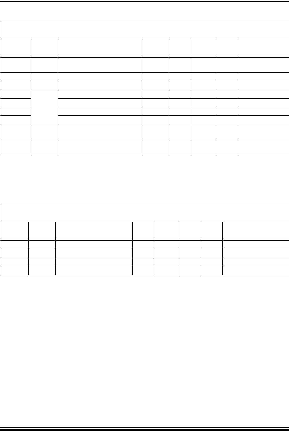
TABLE 29-16: DIGITAL-TO-ANALOG CONVERTER (DAC) SPECIFICATIONS
(1)
Operating Conditions (unless otherwise stated)
V
DD = 3.0V, TA = 25°C
Param.
No.
Sym. Characteristics Min. Typ. Max. Units Comments
CM01 V
IOFF Input Offset Voltage — ±7.5 ±60 mV CxSP = 1,
V
ICM = VDD/2
CM02 VICM Input Common Mode Voltage 0 — VDD V
CM03 C
MRR Common Mode Rejection Ration — 50 — dB
CM04A
T
RESP
(2)
Response Time Rising Edge — 400 800 ns CxSP = 1
CM04B Response Time Falling Edge — 200 400 ns CxSP = 1
CM04C Response Time Rising Edge — 1200 — ns CxSP = 0
CM04D Response Time Falling Edge — 550 — ns CxSP = 0
CM05* T
MC2OV Comparator Mode Change to
Output Valid
——10s
CM06 C
HYSTER Comparator Hysteresis — 25 — mV CxHYS = 1,
CxSP = 1
* These parameters are characterized but not tested.
Note 1: See Section 30.0 “DC and AC Characteristics Graphs and Charts” for operating characterization.
2: Response time measured with one comparator input at V
DD/2, while the other input transitions from VSS to
V
DD.
Operating Conditions (unless otherwise stated)
V
DD = 3.0V, TA = 25°C
Param.
No.
Sym. Characteristics Min. Typ. Max. Units Comments
DAC01* C
LSB Step Size — VDD/32 — V
DAC02* CACC Absolute Accuracy — — 1/2 LSb
DAC03* CR Unit Resistor Value (R) — 5K —
DAC04* C
ST Settling Time
(2)
——10s
* These parameters are characterized but not tested.
Note 1: See Section 30.0 “DC and AC Characteristics Graphs and Charts” for operating characterization.
2: Settling time measured while DACR<4:0> transitions from ‘0000’ to ‘1111’.