
Datasheet


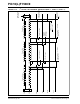
Table Of Contents
- 20-Pin Flash, 8-Bit Microcontrollers with XLP Technology
- PIC12(L)F1501/PIC16(L)F150X Family Types
- Pin Diagrams
- Pin Allocation Table
- TABLE 1: 20-Pin Allocation Table (PIC16(L)F1508/9)
- Table of Contents
- 1.0 Device Overview
- 2.0 Enhanced Mid-Range CPU
- 3.0 Memory Organization
- TABLE 3-1: Device Sizes and Addresses
- FIGURE 3-1: Program Memory Map And Stack For PIC16(L)F1508
- FIGURE 3-2: Program Memory Map And Stack For PIC16(L)F1509
- TABLE 3-2: Core Registers
- FIGURE 3-3: Banked Memory Partitioning
- TABLE 3-3: PIC16(L)F1509 Memory Map, Bank 1-7
- TABLE 3-4: PIC16(L)F1508 Memory Map, Bank 1-7
- TABLE 3-5: PIC16(L)F1508/9 Memory Map, Bank 8-23
- 3.1 Program Memory Organization
- FIGURE 3-11: Linear Data Memory Map
- TABLE 3-6: PIC16(L)F1508/9 Memory Map, Bank 24-31
- TABLE 3-7: PIC16(L)F1508/9 Memory Map, Bank 30-31
- TABLE 3-8: Core Function Registers Summary
- TABLE 3-9: Special Function Register Summary
- FIGURE 3-4: Loading of PC in Different Situations
- FIGURE 3-5: Accessing the Stack Example 1
- FIGURE 3-6: Accessing the Stack Example 2
- FIGURE 3-7: Accessing the Stack Example 3
- FIGURE 3-8: Accessing the Stack Example 4
- FIGURE 3-9: Indirect Addressing
- FIGURE 3-10: Traditional Data Memory Map
- FIGURE 3-12: Program Flash Memory Map
- 4.0 Device Configuration
- 4.1 Configuration Words
- 4.2 Register Definitions: Configuration Words
- Register 4-1: CONFIG1: Configuration Word 1
- Register 4-2: CONFIG2: Configuration Word 2
- 4.3 Code Protection
- 4.4 Write Protection
- 4.5 User ID
- 4.6 Device ID and Revision ID
- 4.7 Register Definitions: Device ID
- Register 4-3: DEVID: Device ID Register
- 5.0 Oscillator Module (With Fail-Safe Clock Monitor)
- FIGURE 5-1: Simplified PIC® MCU Clock Source Block Diagram
- FIGURE 5-2: External Clock (EC) Mode Operation
- FIGURE 5-3: Quartz Crystal Operation (LP, XT or HS Mode)
- FIGURE 5-4: Ceramic Resonator Operation (XT or HS Mode)
- FIGURE 5-5: Quartz Crystal Operation (Secondary Oscillator)
- FIGURE 5-6: External RC Modes
- TABLE 5-1: Peripheral Clock Sources
- FIGURE 5-7: Internal Oscillator Switch Timing
- TABLE 5-2: OSTS Bit Definition
- TABLE 5-3: Oscillator Switching Delays
- FIGURE 5-8: Two-Speed Start-up
- FIGURE 5-9: FSCM Block Diagram
- FIGURE 5-10: FSCM Timing Diagram
- TABLE 5-4: Summary of Registers Associated with Clock Sources
- 5.1 Overview
- TABLE 5-5: Summary of Configuration Word with Clock Sources
- 6.0 Resets
- FIGURE 6-1: Simplified Block Diagram of On-Chip Reset Circuit
- TABLE 6-1: BOR Operating Modes
- FIGURE 6-2: Brown-out Situations
- TABLE 6-2: MCLR Configuration
- FIGURE 6-3: Reset Start-up Sequence
- TABLE 6-3: Reset Status Bits and Their Significance
- TABLE 6-4: Reset Condition for Special Registers
- TABLE 6-5: Summary of Registers Associated with Resets
- TABLE 6-6: Summary of Configuration Word with Resets
- 7.0 Interrupts
- FIGURE 7-1: Interrupt Logic
- FIGURE 7-2: Interrupt Latency
- FIGURE 7-3: INT Pin Interrupt Timing
- 7.3 Interrupts During Sleep
- 7.4 INT Pin
- 7.5 Automatic Context Saving
- 7.6 Register Definitions: Interrupt Control
- Register 7-1: INTCON: Interrupt Control Register
- Register 7-2: PIE1: Peripheral Interrupt Enable Register 1
- Register 7-3: PIE2: Peripheral Interrupt Enable Register 2
- Register 7-4: PIE3: Peripheral Interrupt Enable Register 3
- Register 7-5: PIR1: Peripheral Interrupt Request Register 1
- Register 7-6: PIR2: Peripheral Interrupt Request Register 2
- Register 7-7: PIR3: Peripheral Interrupt Request Register 3
- TABLE 7-1: Summary of Registers Associated with Interrupts
- 8.0 Power-Down Mode (Sleep)
- 9.0 Watchdog Timer (WDT)
- 10.0 Flash Program Memory Control
- TABLE 10-1: Flash Memory Organization by Device
- FIGURE 10-1: Flash Program Memory Read Flowchart
- FIGURE 10-2: Flash Program Memory Read Cycle Execution
- FIGURE 10-3: Flash Program Memory Unlock Sequence Flowchart
- FIGURE 10-4: Flash Program Memory Erase Flowchart
- FIGURE 10-5: Block Writes to Flash Program Memory with 32 Write latches
- FIGURE 10-6: Flash Program Memory Write Flowchart
- FIGURE 10-7: Flash Program Memory Modify Flowchart
- TABLE 10-2: User ID, Device ID and Configuration Word Access (CFGS = 1)
- 10.1 PMADRL and PMADRH Registers
- 10.2 Flash Program Memory Overview
- FIGURE 10-8: Flash Program Memory Verify Flowchart
- 10.6 Register Definitions: Flash Program Memory Control
- Register 10-1: PMDATL: Program Memory Data Low Byte Register
- Register 10-2: PMDATH: Program Memory Data High Byte Register
- Register 10-3: PMADRL: Program Memory Address Low Byte Register
- Register 10-4: PMADRH: Program Memory Address High Byte Register
- Register 10-5: PMCON1: Program Memory Control 1 Register
- Register 10-6: PMCON2: Program Memory Control 2 Register
- TABLE 10-3: Summary of Registers Associated with Flash Program Memory
- TABLE 10-4: Summary of Configuration Word with Flash Program Memory
- 11.0 I/O Ports
- TABLE 11-1: Port Availability Per Device
- FIGURE 11-1: Generic I/O Port Operation
- TABLE 11-2: PORTA Output Priority
- TABLE 11-3: Summary of Registers Associated with PORTA
- TABLE 11-4: Summary of Configuration Word with PORTA
- TABLE 11-5: PORTB Output Priority
- TABLE 11-6: Summary of Registers Associated with PORTB
- TABLE 11-7: Summary of Configuration Word with PORTB
- TABLE 11-8: PORTC Output Priority
- TABLE 11-9: Summary of Registers Associated with PORTC
- 12.0 Interrupt-On-Change
- FIGURE 12-1: Interrupt-On-Change Block Diagram (PORTA Example)
- 12.6 Register Definitions: Interrupt-on-Change Control
- Register 12-1: IOCAP: Interrupt-on-Change PORTA Positive Edge Register
- Register 12-2: IOCAN: Interrupt-on-Change PORTA Negative Edge Register
- Register 12-3: IOCAF: Interrupt-on-Change PORTA Flag Register
- Register 12-4: IOCBP: Interrupt-on-Change PORTB Positive Edge Register
- Register 12-5: IOCBN: Interrupt-on-Change PORTB Negative Edge Register
- Register 12-6: IOCBF: Interrupt-on-Change PORTB Flag Register
- TABLE 12-1: Summary of Registers Associated with Interrupt-on-Change
- 12.1 Enabling the Module
- 12.2 Individual Pin Configuration
- 12.3 Interrupt Flags
- 12.4 Clearing Interrupt Flags
- EXAMPLE 12-1: Clearing Interrupt Flags (PORTA Example)
- 12.5 Operation in Sleep
- FIGURE 12-1: Interrupt-On-Change Block Diagram (PORTA Example)
- 13.0 Fixed Voltage Reference (FVR)
- 14.0 Temperature Indicator Module
- 15.0 Analog-to-Digital Converter (ADC) Module
- FIGURE 15-1: ADC Block Diagram
- TABLE 15-1: ADC Clock Period (Tad) Vs. Device Operating Frequencies
- FIGURE 15-2: Analog-to-Digital Conversion Tad Cycles
- FIGURE 15-3: 10-Bit ADC Conversion Result Format
- TABLE 15-2: Auto-Conversion Sources
- EXAMPLE 15-1: ADC Conversion
- 15.3 Register Definitions: ADC Control
- Register 15-1: ADCON0: ADC Control Register 0
- Register 15-2: ADCON1: ADC Control Register 1
- Register 15-3: ADCON2: ADC Control Register 2
- Register 15-4: ADRESH: ADC Result Register High (ADRESH) ADFM = 0
- Register 15-5: ADRESL: ADC Result Register Low (ADRESL) ADFM = 0
- Register 15-6: ADRESH: ADC Result Register High (ADRESH) ADFM = 1
- Register 15-7: ADRESL: ADC Result Register Low (ADRESL) ADFM = 1
- 15.4 ADC Acquisition Requirements
- EQUATION 15-1: Acquisition Time Example
- FIGURE 15-4: Analog Input Model
- FIGURE 15-5: ADC Transfer Function
- TABLE 15-3: Summary of Registers Associated with ADC
- 16.0 5-Bit Digital-to-Analog Converter (DAC) Module
- FIGURE 16-1: Digital-to-Analog Converter Block Diagram
- 16.1 Output Voltage Selection
- 16.2 Ratiometric Output Level
- 16.3 DAC Voltage Reference Output
- 16.4 Operation During Sleep
- 16.5 Effects of a Reset
- EQUATION 16-1: DAC Output Voltage
- 16.6 Register Definitions: DAC Control
- Register 16-1: DACxCON0: Voltage Reference Control Register 0
- Register 16-2: DACxCON1: Voltage Reference Control Register 1
- TABLE 16-1: Summary of Registers Associated with the DAC Module
- FIGURE 16-1: Digital-to-Analog Converter Block Diagram
- 17.0 Comparator Module
- TABLE 17-1: Available Comparators
- FIGURE 17-1: Comparator Module Simplified Block Diagram
- FIGURE 17-2: Single Comparator
- TABLE 17-2: Comparator Output State vs. Input Conditions
- FIGURE 17-3: Analog Input Model
- FIGURE 17-4: Analog Input Model
- 17.4 Comparator Hysteresis
- 17.5 Timer1 Gate Operation
- 17.6 Comparator Interrupt
- 17.7 Comparator Response Time
- 17.8 Register Definitions: Comparator Control
- Register 17-1: CMxCON0: Comparator Cx Control Register 0
- Register 17-2: CMxCON1: Comparator Cx Control Register 1
- Register 17-3: CMOUT: Comparator Output Register
- TABLE 17-3: Summary of Registers Associated with Comparator Module
- 17.1 Comparator Overview
- 18.0 Timer0 Module
- 19.0 Timer1 Module with Gate Control
- FIGURE 19-1: Timer1 Block Diagram
- TABLE 19-1: Timer1 Enable Selections
- TABLE 19-2: Clock Source Selections
- TABLE 19-3: Timer1 Gate Enable Selections
- TABLE 19-4: Timer1 Gate Sources
- FIGURE 19-2: Timer1 Incrementing Edge
- FIGURE 19-3: Timer1 Gate Enable Mode
- FIGURE 19-4: Timer1 Gate Toggle Mode
- FIGURE 19-5: Timer1 Gate Single-Pulse Mode
- FIGURE 19-6: Timer1 Gate Single-Pulse and Toggle Combined Mode
- TABLE 19-5: Summary of Registers Associated with Timer1
- 20.0 Timer2 Module
- 21.0 Master Synchronous Serial Port (MSSP) Module
- FIGURE 21-1: MSSP Block Diagram (SPI mode)
- FIGURE 21-2: MSSPx Block Diagram (I2C™ Master mode)
- FIGURE 21-3: MSSP Block Diagram (I2C™ Slave mode)
- FIGURE 21-4: SPI Master and Multiple Slave Connection
- FIGURE 21-5: SPI Master/Slave Connection
- FIGURE 21-6: SPI Mode Waveform (Master Mode)
- FIGURE 21-7: SPI Daisy-Chain Connection
- FIGURE 21-8: Slave Select Synchronous Waveform
- FIGURE 21-9: SPI Mode Waveform (Slave Mode With CKE = 0)
- FIGURE 21-10: SPI Mode Waveform (SLAve Mode With CKE = 1)
- 21.1 MSSP Module Overview
- TABLE 21-1: Summary of Registers Associated with SPI Operation
- FIGURE 21-11: I2C Master/ Slave Connection
- TABLE 21-2: I2C Bus terms
- FIGURE 21-12: I2C Start and Stop Conditions
- FIGURE 21-13: I2C Restart Condition
- FIGURE 21-14: I2C Slave, 7-bit Address, Reception (SEN = 0, AHEN = 0, DHEN = 0)
- FIGURE 21-15: I2C Slave, 7-bit Address, Reception (SEN = 1, AHEN = 0, DHEN = 0)
- FIGURE 21-16: I2C Slave, 7-bit Address, Reception (SEN = 0, AHEN = 1, DHEN = 1)
- FIGURE 21-17: I2C Slave, 7-bit Address, Reception (SEN = 1, AHEN = 1, DHEN = 1)
- FIGURE 21-18: I2C Slave, 7-bit Address, Transmission (AHEN = 0)
- FIGURE 21-19: I2C Slave, 7-bit Address, Transmission (AHEN = 1)
- FIGURE 21-20: I2C Slave, 10-bit Address, Reception (SEN = 1, AHEN = 0, DHEN = 0)
- FIGURE 21-21: I2C Slave, 10-bit Address, Reception (SEN = 0, AHEN = 1, DHEN = 0)
- FIGURE 21-22: I2C Slave, 10-bit Address, Transmission (SEN = 0, AHEN = 0, DHEN = 0)
- FIGURE 21-23: Clock Synchronization Timing
- FIGURE 21-24: Slave Mode General Call Address Sequence
- FIGURE 21-25: Baud Rate Generator Timing with Clock Arbitration
- FIGURE 21-26: First Start Bit Timing
- FIGURE 21-27: Repeat Start Condition Waveform
- FIGURE 21-28: I2C Master Mode Waveform (Transmission, 7 or 10-bit Address)
- FIGURE 21-29: I2C Master Mode Waveform (Reception, 7-bit Address)
- FIGURE 21-30: Acknowledge Sequence Waveform
- FIGURE 21-31: Stop Condition Receive or Transmit Mode
- FIGURE 21-32: Bus Collision Timing for Transmit and Acknowledge
- FIGURE 21-33: Bus Collision During Start Condition (SDAx Only)
- FIGURE 21-34: Bus Collision During Start Condition (SCLx = 0)
- FIGURE 21-35: BRG Reset Due to SDA Arbitration During Start Condition
- FIGURE 21-36: Bus Collision During a Repeated Start Condition (Case 1)
- FIGURE 21-37: Bus Collision During Repeated Start Condition (Case 2)
- FIGURE 21-38: Bus Collision During a Stop Condition (Case 1)
- FIGURE 21-39: Bus Collision During a Stop Condition (Case 2)
- TABLE 21-3: Summary of Registers Associated with I2C™ Operation
- FIGURE 21-40: Baud Rate Generator Block Diagram
- TABLE 21-4: MSSP Clock Rate w/BRG
- 21.8 Register Definitions: MSSP Control
- Register 21-1: SSPxSTAT: SSP STATUS Register
- Register 21-2: SSPxCON1: SSP Control Register 1
- Register 21-3: SSPxCON2: SSP Control Register 2(1)
- Register 21-4: SSPxCON3: SSP Control Register 3
- Register 21-5: SSPxMSK: SSP Mask Register
- Register 21-6: SSPxADD: MSSP Address and Baud Rate Register (I2C Mode)
- 22.0 Enhanced Universal Synchronous Asynchronous Receiver Transmitter (EUSART)
- FIGURE 22-1: EUSART Transmit Block Diagram
- FIGURE 22-2: EUSART Receive Block Diagram
- FIGURE 22-3: Asynchronous Transmission
- FIGURE 22-4: Asynchronous Transmission (Back-to-Back)
- TABLE 22-1: Summary of Registers Associated with Asynchronous Transmission
- FIGURE 22-5: Asynchronous Reception
- TABLE 22-2: Summary of Registers Associated with Asynchronous Reception
- 22.2 Clock Accuracy with Asynchronous Operation
- 22.3 Register Definitions: EUSART Control
- Register 22-1: TXSTA: Transmit Status and Control Register
- Register 22-2: RCSTA: Receive Status and Control Register
- Register 22-3: BAUDCON: Baud Rate Control Register
- 22.4 EUSART Baud Rate Generator (BRG)
- EXAMPLE 22-1: Calculating Baud Rate Error
- TABLE 22-3: Baud Rate Formulas
- TABLE 22-4: Summary of Registers Associated with the Baud Rate Generator
- TABLE 22-5: BAUD Rates for Asynchronous Modes
- TABLE 22-6: BRG Counter Clock Rates
- FIGURE 22-6: Automatic Baud Rate Calibration
- FIGURE 22-7: Auto-Wake-up Bit (WUE) Timing During Normal Operation
- FIGURE 22-8: Auto-Wake-up Bit (WUE) Timings During Sleep
- FIGURE 22-9: Send Break Character Sequence
- FIGURE 22-10: Synchronous Transmission
- FIGURE 22-11: Synchronous Transmission (Through TXEN)
- TABLE 22-7: Summary of Registers Associated with Synchronous Master Transmission
- FIGURE 22-12: Synchronous Reception (Master Mode, SREN)
- TABLE 22-8: Summary of Registers Associated with Synchronous Master Reception
- TABLE 22-9: Summary of Registers Associated with Synchronous Slave Transmission
- TABLE 22-10: Summary of Registers Associated with Synchronous Slave Reception
- 23.0 Pulse Width Modulation (PWM) Module
- 24.0 Configurable Logic Cell (CLC)
- FIGURE 24-1: Digital-to-Analog Converter Block Diagram
- TABLE 24-1: CLCx Data Input Selection
- TABLE 24-2: Data Gating Logic
- FIGURE 24-2: Input Data Selection and Gating
- FIGURE 24-3: Programmable Logic Functions
- 24.6 Register Definitions: CLC Control
- Register 24-1: CLCxCON: Configurable Logic Cell Control Register
- Register 24-2: CLCxPOL: Signal Polarity Control Register
- Register 24-3: CLCxSEL0: Multiplexer Data 1 and 2 Select Register
- Register 24-4: CLCxSEL1: Multiplexer Data 3 and 4 Select Register
- Register 24-5: CLCxGLS0: Gate 1 Logic Select Register
- Register 24-6: CLCxGLS1: Gate 2 Logic Select Register
- Register 24-7: CLCxGLS2: Gate 3 Logic Select Register
- Register 24-8: CLCxGLS3: Gate 4 Logic Select Register
- Register 24-9: CLCDATA: CLC Data Output
- TABLE 24-3: Summary of Registers Associated with CLCx
- 25.0 Numerically Controlled Oscillator (NCO) Module
- FIGURE 25-1: Numerically Controlled Oscillator (NCOx) Module Simplified Block Diagram
- FIGURE 25-2: NCO – Fixed Duty Cycle (FDC) and Pulse Frequency Mode (PFM) Output Operation Diagram
- 25.9 Register Definitions: NCOx Control Registers
- Register 25-1: NCOxCON: NCOx Control Register
- Register 25-2: NCOxCLK: NCOx Input Clock Control Register
- Register 25-3: NCOxACCL: NCOx Accumulator Register – Low Byte
- Register 25-4: NCOxACCH: NCOx Accumulator Register – High Byte
- Register 25-5: NCOxACCU: NCOx Accumulator Register – Upper Byte
- Register 25-6: NCOxINCL: NCOx Increment Register – Low Byte(1)
- Register 25-7: NCOxINCH: NCOx Increment Register – High Byte(1)
- TABLE 25-1: Summary of Registers Associated with NCOx
- 25.1 NCOx Operation
- EQUATION 25-1:
- 26.0 Complementary Waveform Generator (CWG) Module
- TABLE 26-1: Selectable Input Sources
- FIGURE 26-1: Simplified CWG Block Diagram
- FIGURE 26-2: Typical CWG Operation with PWM1 (No Auto-shutdown)
- FIGURE 26-3: Dead-Band Operation, CWGxDBR = 01H, CWGxDBF = 02H
- FIGURE 26-4: Dead-Band Operation, CWGxDBR = 03H, CWGxDBF = 04H, Source Shorter Than Dead Band
- FIGURE 26-5: Shutdown Functionality, Auto-Restart Disabled (GxARSEN = 0,GxASDLA = 01, GxASDLB = 01)
- FIGURE 26-6: Shutdown Functionality, Auto-Restart Enabled (GxARSEN = 1,GxASDLA = 01, GxASDLB = 01)
- 26.12 Register Definitions: CWG Control
- Register 26-1: CWGxCON0: CWG Control Register 0
- Register 26-2: CWGxCON1: CWG Control Register 1
- Register 26-3: CWGXCON2: CWG Control Register 2
- Register 26-4: CWGxDBR: Complementary Waveform Generator (CWGx) Rising Dead-Band Count Register
- Register 26-5: CWGxdbf: Complementary Waveform Generator (CWGx) Falling Dead-Band Count Register
- 26.1 Fundamental Operation
- 26.2 Clock Source
- 26.3 Selectable Input Sources
- TABLE 26-2: Summary of Registers Associated with CWG
- 27.0 In-Circuit Serial Programming™ (ICSP™)
- 28.0 Instruction Set Summary
- 29.0 Electrical Specifications
- FIGURE 29-13: ADC Conversion Timing (ADC Clock from FRC)
- FIGURE 29-15: USART Synchronous Receive (Master/Slave) Timing
- TABLE 29-18: USART Synchronous Receive Requirements
- FIGURE 29-16: SPI Master Mode Timing (CKE = 0, SMP = 0)
- FIGURE 29-17: SPI Master Mode Timing (CKE = 1, SMP = 1)
- FIGURE 29-18: SPI Slave Mode Timing (CKE = 0)
- FIGURE 29-19: SPI Slave Mode Timing (CKE = 1)
- TABLE 29-19: SPI Mode requirements
- FIGURE 29-20: I2C™ Bus Start/Stop Bits Timing
- TABLE 29-20: I2C™ Bus Start/Stop Bits Requirements
- FIGURE 29-21: I2C™ Bus Data Timing
- TABLE 29-14: ADC Conversion Requirements
- TABLE 29-15: Comparator Specifications(1)
- TABLE 29-16: Digital-to-Analog Converter (DAC) Specifications(1)
- FIGURE 29-14: USART Synchronous Transmission (Master/Slave) Timing
- TABLE 29-17: USART Synchronous Transmission Requirements
- FIGURE 29-1: Voltage Frequency Graph, -40°C £ Ta £ +125°C, PIC16F1508/9 only
- FIGURE 29-2: Voltage Frequency Graph, -40°C £ Ta £ +125°C, PIC16LF1508/9 only
- TABLE 29-1: Supply Voltage
- FIGURE 29-3: POR and POR Rearm with Slow Rising Vdd
- TABLE 29-2: Supply Current (Idd)(1,2)
- TABLE 29-3: Power-Down Currents (Ipd)(1,2)
- TABLE 29-4: I/O Ports
- TABLE 29-5: Memory Programming Specifications
- TABLE 29-6: Thermal Characteristics
- FIGURE 29-4: Load Conditions
- FIGURE 29-5: Clock Timing
- TABLE 29-7: Clock Oscillator Timing Requirements
- TABLE 29-8: Oscillator Parameters
- 29.1 Absolute Maximum Ratings(†)
- 29.2 Standard Operating Conditions
- FIGURE 29-6: HFINTOSC Frequency Accuracy Over Vdd and Temperature
- FIGURE 29-7: CLKOUT and I/O Timing
- TABLE 29-9: CLKOUT and I/O Timing Parameters
- FIGURE 29-8: Reset, Watchdog Timer, Oscillator Start-up Timer and Power-up Timer Timing
- TABLE 29-10: Reset, Watchdog Timer, Oscillator Start-up Timer, Power-up Timer and Brown-Out Reset Parameters
- FIGURE 29-9: Brown-Out Reset Timing and Characteristics
- FIGURE 29-10: Timer0 and Timer1 External Clock Timings
- TABLE 29-11: Timer0 and Timer1 External Clock Requirements
- FIGURE 29-11: CLC Propagation Timing
- TABLE 29-12: Configuration Logic Cell (CLC) Characteristics
- TABLE 29-13: Analog-to-Digital Converter (ADC) Characteristics(1,2,3)
- FIGURE 29-12: ADC Conversion Timing (ADC Clock Fosc-based)
- FIGURE 29-13: ADC Conversion Timing (ADC Clock from FRC)
- 30.0 DC and AC Characteristics Graphs and Charts
- FIGURE 30-1: Idd, LP Oscillator, Fosc = 32 kHz, PIC16LF1508/9 ONLY
- FIGURE 30-2: Idd, LP Oscillator, Fosc = 32 kHz, PIC16F1508/9 ONLY
- FIGURE 30-3: Idd Typical, XT and EXTRC Oscillator, PIC16LF1508/9 ONLY
- FIGURE 30-4: Idd Maximum, XT and EXTRC Oscillator, PIC16LF1508/9 ONLY
- FIGURE 30-5: Idd Typical, XT and EXTRC Oscillator, PIC16F1508/9 ONLY
- FIGURE 30-6: Idd Maximum, XT and EXTRC Oscillator, PIC16F1508/9 ONLY
- FIGURE 30-7: Idd, External Clock (ECL), Low-Power Mode, Fosc = 32 kHz, PIC16LF1508/9 ONLY
- FIGURE 30-8: Idd, External Clock (ECL), Low-Power Mode, Fosc = 32 kHz, PIC16F1508/9 ONLY
- FIGURE 30-9: Idd, External Clock (ECL), Low-Power Mode, Fosc = 500 kHz, PIC16LF1508/9 ONLY
- FIGURE 30-10: Idd, External Clock (ECL), Low-Power Mode, Fosc = 500 kHz, PIC16F1508/9 ONLY
- FIGURE 30-13: Idd Typical, External Clock (ECM), Medium-Power Mode, PIC16F1508/9 ONLY
- FIGURE 30-14: Idd Maximum, External Clock (ECM), Medium-Power Mode, PIC16F1508/9 ONLY
- FIGURE 30-15: Idd Typical, External Clock (ECH), High-Power Mode, PIC16LF1508/9 ONLY
- FIGURE 30-16: Idd Maximum, External Clock (ECH), High-Power Mode, PIC16LF1508/9 ONLY
- FIGURE 30-17: Idd Typical, External Clock (ECH), High-Power Mode, PIC16F1508/9 ONLY
- FIGURE 30-18: Idd Maximum, External Clock (ECH), High-Power Mode, PIC16F1508/9 ONLY
- FIGURE 30-12: Idd Maximum, External Clock (ECM), Medium-Power Mode, PIC16LF1508/9 ONLY
- FIGURE 30-11: Idd Typical, External Clock (ECM), Medium-Power Mode, PIC16LF1508/9 ONLY
- FIGURE 30-19: Idd, LFINTOSC, Fosc = 31 kHz, PIC16LF1508/9 Only
- FIGURE 30-20: Idd, LFINTOSC, Fosc = 31 kHz, PIC16F1508/9 Only
- FIGURE 30-21: Idd, MFINTOSC, Fosc = 500 kHz, PIC16LF1508/9 ONLY
- FIGURE 30-22: Idd, MFINTOSC, Fosc = 500 kHz, PIC16F1508/9 ONLY
- FIGURE 30-23: Idd Typical, HFINTOSC, PIC16LF1508/9 ONLY
- FIGURE 30-24: Idd Maximum, HFINTOSC, PIC16LF1508/9 ONLY
- FIGURE 30-25: Idd Typical, HFINTOSC, PIC16F1508/9 ONLY
- FIGURE 30-26: Idd Maximum, HFINTOSC, PIC16F1508/9 ONLY
- FIGURE 30-27: Idd Typical, HS OScillator, PIC16LF1508/9 ONLY
- FIGURE 30-28: Idd Maximum, HS Oscillator, PIC16LF1508/9 ONLY
- FIGURE 30-29: Idd Typical, HS Oscillator, PIC16F1508/9 ONLY
- FIGURE 30-30: Idd Maximum, HS Oscillator, PIC16F1508/9 ONLY
- FIGURE 30-31: Ipd Base, Low-Power Sleep Mode, PIC16LF1508/9 ONly
- FIGURE 30-32: Ipd Base, Low-Power Sleep Mode, VREGPM = 1, PIC16F1508/9 ONLy
- FIGURE 30-33: Ipd, Watchdog Timer (WDT), PIC16LF1508/9 ONLy
- FIGURE 30-34: Ipd, Watchdog Timer (WDT), PIC16F1508/9 ONLy
- FIGURE 30-35: Ipd, Fixed Voltage Reference (FVR), PIC16LF1508/9 ONLy
- FIGURE 30-36: Ipd, Fixed Voltage Reference (FVR), PIC16F1508/9 ONLy
- FIGURE 30-37: Ipd, Brown-Out Reset (BOR), BORV = 0, PIC16LF1508/9 ONLY
- FIGURE 30-38: Ipd, Brown-Out Reset (BOR), BORV = 1, PIC16LF1508/9 Only
- FIGURE 30-39: Ipd, Brown-Out Reset (BOR), BORV = 0, PIC16F1508/9 Only
- FIGURE 30-40: Ipd, Brown-Out Reset (BOR), BORV = 1, PIC16F1508/9 Only
- FIGURE 30-41: Ipd, Secondary Oscillator, Fosc = 32 kHz, PIC16LF1508/9 Only
- FIGURE 30-42: Ipd, Secondary Oscillator, Fosc = 32 kHz, PIC16F1508/9 Only
- FIGURE 30-43: Ipd, Comparator, Low-Power Mode (CxSP = 0), PIC16LF1508/9 Only
- FIGURE 30-44: Ipd, Comparator, Low-Power Mode (CxSP = 0), PIC16F1508/9 Only
- FIGURE 30-45: Ipd, Comparator, Normal-Power Mode (CxSP = 1), PIC16LF1508/9 Only
- FIGURE 30-46: Ipd, Comparator, Normal-Power Mode (CxSP = 1), PIC16F1508/9 Only
- FIGURE 30-47: Voh vs. Ioh over Temperature, Vdd = 5.5V, PIC16F1508/9 Only
- FIGURE 30-48: Vol vs. Iol over Temperature, Vdd = 5.5V, PIC16F1508/9 Only
- FIGURE 30-49: Voh vs. Ioh over Temperature, Vdd = 3.0V
- FIGURE 30-50: Vol vs. Iol over Temperature, Vdd = 3.0V
- FIGURE 30-51: Voh vs. Ioh over Temperature, Vdd = 1.8V, PIC16LF1508/9 Only
- FIGURE 30-52: Vol vs. Iol over Temperature, Vdd = 1.8V, PIC16LF1508/9 Only
- FIGURE 30-53: POR Release Voltage
- FIGURE 30-54: POR Rearm Voltage, PIC16F1508/9 Only
- FIGURE 30-55: Brown-Out Reset Voltage, BORV = 1, PIC16LF1508/9 Only
- FIGURE 30-56: Brown-Out Reset Hysteresis, BORV = 1, PIC16LF1508/9 Only
- FIGURE 30-57: Brown-Out Reset Voltage, BORV = 1, PIC16F1508/9 Only
- FIGURE 30-58: Brown-Out Reset Hysteresis, BORV = 1, PIC16F1508/9 Only
- FIGURE 30-59: Brown-Out Reset Voltage, BORV = 0
- FIGURE 30-60: Brown-Out Reset Hysteresis, BORV = 0
- FIGURE 30-61: Low-Power Brown-Out Reset Voltage, LPBOR = 0
- FIGURE 30-62: Low-Power Brown-Out Reset Hysteresis, LPBOR = 0
- FIGURE 30-63: WDT Time-Out Period
- FIGURE 30-64: PWRT Period
- FIGURE 30-65: FVR Stabilization Period
- FIGURE 30-66: Comparator Hysteresis, Normal-Power Mode (CxSP = 1, CxHYS = 1)
- FIGURE 30-67: Comparator Hysteresis, Low-Power Mode (CxSP = 0, CxHYS = 1)
- FIGURE 30-68: Comparator Response Time, Normal-Power Mode (CxSP = 1)
- FIGURE 30-69: Comparator Response Time Over Temperature, Normal-Power Mode (CxSP = 1)
- FIGURE 30-70: Comparator Input Offset at 25°C, Normal-Power Mode (CxSP = 1), PIC16F1508/9 Only
- FIGURE 30-71: LFINTOSC Frequency Over Vdd and Temperature, PIC16LF1508/9 Only
- FIGURE 30-72: LFINTOSC Frequency Over Vdd and Temperature, PIC16F1508/9 Only
- FIGURE 30-73: HFINTOSC Accuracy Over Temperature, Vdd = 1.8V, PIC16LF1508/9 Only
- FIGURE 30-74: HFINTOSC Accuracy Over Temperature, 2.3V £ Vdd £ 5.5V
- FIGURE 30-75: Sleep Mode, Wake Period with HFINTOSC Source, PIC16LF1508/9 Only
- FIGURE 30-76: Low-Power Sleep Mode, Wake Period with HFINTOSC Source, VREGPM = 1, PIC16F1508/9 Only
- FIGURE 30-77: Sleep Mode, Wake Period with HFINTOSC Source, VREGPM = 0, PIC16F1508/9 Only
- 31.0 Development Support
- 31.1 MPLAB X Integrated Development Environment Software
- 31.2 MPLAB XC Compilers
- 31.3 MPASM Assembler
- 31.4 MPLINK Object Linker/ MPLIB Object Librarian
- 31.5 MPLAB Assembler, Linker and Librarian for Various Device Families
- 31.6 MPLAB X SIM Software Simulator
- 31.7 MPLAB REAL ICE In-Circuit Emulator System
- 31.8 MPLAB ICD 3 In-Circuit Debugger System
- 31.9 PICkit 3 In-Circuit Debugger/ Programmer
- 31.10 MPLAB PM3 Device Programmer
- 31.11 Demonstration/Development Boards, Evaluation Kits, and Starter Kits
- 31.12 Third-Party Development Tools
- 32.0 Packaging Information
- Appendix A: Data Sheet Revision History
- Product ID System
- Trademarks
- Worldwide Sales and Service

2011-2013 Microchip Technology Inc. DS40001609C-page 197
PIC16(L)F1508/9
21.4.9 ACKNOWLEDGE SEQUENCE
The ninth SCLx pulse for any transferred byte in I
2
C is
dedicated as an Acknowledge. It allows receiving
devices to respond back to the transmitter by pulling
the SDAx line low. The transmitter must release con-
trol of the line during this time to shift in the response.
The Acknowledge (ACK
) is an active-low signal, pull-
ing the SDAx line low indicated to the transmitter that
the device has received the transmitted data and is
ready to receive more.
The result of an ACK
is placed in the ACKSTAT bit of
the SSPxCON2 register.
Slave software, when the AHEN and DHEN bits are
set, allow the user to set the ACK
value sent back to
the transmitter. The ACKDT bit of the SSPxCON2 reg-
ister is set/cleared to determine the response.
Slave hardware will generate an ACK
response if the
AHEN and DHEN bits of the SSPxCON3 register are
clear.
There are certain conditions where an ACK
will not be
sent by the slave. If the BF bit of the SSPxSTAT regis-
ter or the SSPOV bit of the SSPxCON1 register are
set when a byte is received.
When the module is addressed, after the eighth falling
edge of SCLx on the bus, the ACKTIM bit of the
SSPxCON3 register is set. The ACKTIM bit indicates
the acknowledge time of the active bus. The ACKTIM
Status bit is only active when the AHEN bit or DHEN
bit is enabled.
21.5 I
2
C Slave Mode Operation
The MSSP Slave mode operates in one of four modes
selected in the SSPM bits of SSPxCON1 register. The
modes can be divided into 7-bit and 10-bit Addressing
mode. 10-bit Addressing modes operate the same as
7-bit with some additional overhead for handling the
larger addresses.
Modes with Start and Stop bit interrupts operate the
same as the other modes with SSPxIF additionally
getting set upon detection of a Start, Restart, or Stop
condition.
21.5.1 SLAVE MODE ADDRESSES
The SSPxADD register (Register 21-6) contains the
Slave mode address. The first byte received after a
Start or Restart condition is compared against the
value stored in this register. If the byte matches, the
value is loaded into the SSPxBUF register and an
interrupt is generated. If the value does not match, the
module goes idle and no indication is given to the soft-
ware that anything happened.
The SSP Mask register (Register 21-5) affects the
address matching process. See Section 21.5.9
“SSPx Mask Register” for more information.
21.5.1.1 I
2
C Slave 7-bit Addressing Mode
In 7-bit Addressing mode, the LSb of the received data
byte is ignored when determining if there is an address
match.
21.5.1.2 I
2
C Slave 10-bit Addressing Mode
In 10-bit Addressing mode, the first received byte is
compared to the binary value of ‘1 1 1 1 0 A9 A8 0’. A9
and A8 are the two MSbs of the 10-bit address and
stored in bits 2 and 1 of the SSPxADD register.
After the acknowledge of the high byte the UA bit is set
and SCLx is held low until the user updates SSPxADD
with the low address. The low address byte is clocked
in and all eight bits are compared to the low address
value in SSPxADD. Even if there is not an address
match; SSPxIF and UA are set, and SCLx is held low
until SSPxADD is updated to receive a high byte
again. When SSPxADD is updated the UA bit is
cleared. This ensures the module is ready to receive
the high address byte on the next communication.
A high and low address match as a write request is
required at the start of all 10-bit addressing communi-
cation. A transmission can be initiated by issuing a
Restart once the slave is addressed, and clocking in
the high address with the R/W
bit set. The slave hard-
ware will then acknowledge the read request and pre-
pare to clock out data. This is only valid for a slave
after it has received a complete high and low address
byte match.
21.5.2 SLAVE RECEPTION
When the R/W
bit of a matching received address byte
is clear, the R/W
bit of the SSPxSTAT register is
cleared. The received address is loaded into the
SSPxBUF register and acknowledged.
When the overflow condition exists for a received
address, then not Acknowledge is given. An overflow
condition is defined as either bit BF of the SSPxSTAT
register is set, or bit SSPOV of the SSPxCON1 register
is set. The BOEN bit of the SSPxCON3 register modi-
fies this operation. For more information see
Register 21-4.
An MSSP interrupt is generated for each transferred
data byte. Flag bit, SSPxIF, must be cleared by soft-
ware.
When the SEN bit of the SSPxCON2 register is set,
SCLx will be held low (clock stretch) following each
received byte. The clock must be released by setting
the CKP bit of the SSPxCON1 register, except
sometimes in 10-bit mode. See Section 21.2.3 “SPI
Master Mode” for more detail.