
Datasheet
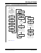


Table Of Contents
- 20-Pin Flash, 8-Bit Microcontrollers with XLP Technology
- PIC12(L)F1501/PIC16(L)F150X Family Types
- Pin Diagrams
- Pin Allocation Table
- TABLE 1: 20-Pin Allocation Table (PIC16(L)F1508/9)
- Table of Contents
- 1.0 Device Overview
- 2.0 Enhanced Mid-Range CPU
- 3.0 Memory Organization
- TABLE 3-1: Device Sizes and Addresses
- FIGURE 3-1: Program Memory Map And Stack For PIC16(L)F1508
- FIGURE 3-2: Program Memory Map And Stack For PIC16(L)F1509
- TABLE 3-2: Core Registers
- FIGURE 3-3: Banked Memory Partitioning
- TABLE 3-3: PIC16(L)F1509 Memory Map, Bank 1-7
- TABLE 3-4: PIC16(L)F1508 Memory Map, Bank 1-7
- TABLE 3-5: PIC16(L)F1508/9 Memory Map, Bank 8-23
- 3.1 Program Memory Organization
- FIGURE 3-11: Linear Data Memory Map
- TABLE 3-6: PIC16(L)F1508/9 Memory Map, Bank 24-31
- TABLE 3-7: PIC16(L)F1508/9 Memory Map, Bank 30-31
- TABLE 3-8: Core Function Registers Summary
- TABLE 3-9: Special Function Register Summary
- FIGURE 3-4: Loading of PC in Different Situations
- FIGURE 3-5: Accessing the Stack Example 1
- FIGURE 3-6: Accessing the Stack Example 2
- FIGURE 3-7: Accessing the Stack Example 3
- FIGURE 3-8: Accessing the Stack Example 4
- FIGURE 3-9: Indirect Addressing
- FIGURE 3-10: Traditional Data Memory Map
- FIGURE 3-12: Program Flash Memory Map
- 4.0 Device Configuration
- 4.1 Configuration Words
- 4.2 Register Definitions: Configuration Words
- Register 4-1: CONFIG1: Configuration Word 1
- Register 4-2: CONFIG2: Configuration Word 2
- 4.3 Code Protection
- 4.4 Write Protection
- 4.5 User ID
- 4.6 Device ID and Revision ID
- 4.7 Register Definitions: Device ID
- Register 4-3: DEVID: Device ID Register
- 5.0 Oscillator Module (With Fail-Safe Clock Monitor)
- FIGURE 5-1: Simplified PIC® MCU Clock Source Block Diagram
- FIGURE 5-2: External Clock (EC) Mode Operation
- FIGURE 5-3: Quartz Crystal Operation (LP, XT or HS Mode)
- FIGURE 5-4: Ceramic Resonator Operation (XT or HS Mode)
- FIGURE 5-5: Quartz Crystal Operation (Secondary Oscillator)
- FIGURE 5-6: External RC Modes
- TABLE 5-1: Peripheral Clock Sources
- FIGURE 5-7: Internal Oscillator Switch Timing
- TABLE 5-2: OSTS Bit Definition
- TABLE 5-3: Oscillator Switching Delays
- FIGURE 5-8: Two-Speed Start-up
- FIGURE 5-9: FSCM Block Diagram
- FIGURE 5-10: FSCM Timing Diagram
- TABLE 5-4: Summary of Registers Associated with Clock Sources
- 5.1 Overview
- TABLE 5-5: Summary of Configuration Word with Clock Sources
- 6.0 Resets
- FIGURE 6-1: Simplified Block Diagram of On-Chip Reset Circuit
- TABLE 6-1: BOR Operating Modes
- FIGURE 6-2: Brown-out Situations
- TABLE 6-2: MCLR Configuration
- FIGURE 6-3: Reset Start-up Sequence
- TABLE 6-3: Reset Status Bits and Their Significance
- TABLE 6-4: Reset Condition for Special Registers
- TABLE 6-5: Summary of Registers Associated with Resets
- TABLE 6-6: Summary of Configuration Word with Resets
- 7.0 Interrupts
- FIGURE 7-1: Interrupt Logic
- FIGURE 7-2: Interrupt Latency
- FIGURE 7-3: INT Pin Interrupt Timing
- 7.3 Interrupts During Sleep
- 7.4 INT Pin
- 7.5 Automatic Context Saving
- 7.6 Register Definitions: Interrupt Control
- Register 7-1: INTCON: Interrupt Control Register
- Register 7-2: PIE1: Peripheral Interrupt Enable Register 1
- Register 7-3: PIE2: Peripheral Interrupt Enable Register 2
- Register 7-4: PIE3: Peripheral Interrupt Enable Register 3
- Register 7-5: PIR1: Peripheral Interrupt Request Register 1
- Register 7-6: PIR2: Peripheral Interrupt Request Register 2
- Register 7-7: PIR3: Peripheral Interrupt Request Register 3
- TABLE 7-1: Summary of Registers Associated with Interrupts
- 8.0 Power-Down Mode (Sleep)
- 9.0 Watchdog Timer (WDT)
- 10.0 Flash Program Memory Control
- TABLE 10-1: Flash Memory Organization by Device
- FIGURE 10-1: Flash Program Memory Read Flowchart
- FIGURE 10-2: Flash Program Memory Read Cycle Execution
- FIGURE 10-3: Flash Program Memory Unlock Sequence Flowchart
- FIGURE 10-4: Flash Program Memory Erase Flowchart
- FIGURE 10-5: Block Writes to Flash Program Memory with 32 Write latches
- FIGURE 10-6: Flash Program Memory Write Flowchart
- FIGURE 10-7: Flash Program Memory Modify Flowchart
- TABLE 10-2: User ID, Device ID and Configuration Word Access (CFGS = 1)
- 10.1 PMADRL and PMADRH Registers
- 10.2 Flash Program Memory Overview
- FIGURE 10-8: Flash Program Memory Verify Flowchart
- 10.6 Register Definitions: Flash Program Memory Control
- Register 10-1: PMDATL: Program Memory Data Low Byte Register
- Register 10-2: PMDATH: Program Memory Data High Byte Register
- Register 10-3: PMADRL: Program Memory Address Low Byte Register
- Register 10-4: PMADRH: Program Memory Address High Byte Register
- Register 10-5: PMCON1: Program Memory Control 1 Register
- Register 10-6: PMCON2: Program Memory Control 2 Register
- TABLE 10-3: Summary of Registers Associated with Flash Program Memory
- TABLE 10-4: Summary of Configuration Word with Flash Program Memory
- 11.0 I/O Ports
- TABLE 11-1: Port Availability Per Device
- FIGURE 11-1: Generic I/O Port Operation
- TABLE 11-2: PORTA Output Priority
- TABLE 11-3: Summary of Registers Associated with PORTA
- TABLE 11-4: Summary of Configuration Word with PORTA
- TABLE 11-5: PORTB Output Priority
- TABLE 11-6: Summary of Registers Associated with PORTB
- TABLE 11-7: Summary of Configuration Word with PORTB
- TABLE 11-8: PORTC Output Priority
- TABLE 11-9: Summary of Registers Associated with PORTC
- 12.0 Interrupt-On-Change
- FIGURE 12-1: Interrupt-On-Change Block Diagram (PORTA Example)
- 12.6 Register Definitions: Interrupt-on-Change Control
- Register 12-1: IOCAP: Interrupt-on-Change PORTA Positive Edge Register
- Register 12-2: IOCAN: Interrupt-on-Change PORTA Negative Edge Register
- Register 12-3: IOCAF: Interrupt-on-Change PORTA Flag Register
- Register 12-4: IOCBP: Interrupt-on-Change PORTB Positive Edge Register
- Register 12-5: IOCBN: Interrupt-on-Change PORTB Negative Edge Register
- Register 12-6: IOCBF: Interrupt-on-Change PORTB Flag Register
- TABLE 12-1: Summary of Registers Associated with Interrupt-on-Change
- 12.1 Enabling the Module
- 12.2 Individual Pin Configuration
- 12.3 Interrupt Flags
- 12.4 Clearing Interrupt Flags
- EXAMPLE 12-1: Clearing Interrupt Flags (PORTA Example)
- 12.5 Operation in Sleep
- FIGURE 12-1: Interrupt-On-Change Block Diagram (PORTA Example)
- 13.0 Fixed Voltage Reference (FVR)
- 14.0 Temperature Indicator Module
- 15.0 Analog-to-Digital Converter (ADC) Module
- FIGURE 15-1: ADC Block Diagram
- TABLE 15-1: ADC Clock Period (Tad) Vs. Device Operating Frequencies
- FIGURE 15-2: Analog-to-Digital Conversion Tad Cycles
- FIGURE 15-3: 10-Bit ADC Conversion Result Format
- TABLE 15-2: Auto-Conversion Sources
- EXAMPLE 15-1: ADC Conversion
- 15.3 Register Definitions: ADC Control
- Register 15-1: ADCON0: ADC Control Register 0
- Register 15-2: ADCON1: ADC Control Register 1
- Register 15-3: ADCON2: ADC Control Register 2
- Register 15-4: ADRESH: ADC Result Register High (ADRESH) ADFM = 0
- Register 15-5: ADRESL: ADC Result Register Low (ADRESL) ADFM = 0
- Register 15-6: ADRESH: ADC Result Register High (ADRESH) ADFM = 1
- Register 15-7: ADRESL: ADC Result Register Low (ADRESL) ADFM = 1
- 15.4 ADC Acquisition Requirements
- EQUATION 15-1: Acquisition Time Example
- FIGURE 15-4: Analog Input Model
- FIGURE 15-5: ADC Transfer Function
- TABLE 15-3: Summary of Registers Associated with ADC
- 16.0 5-Bit Digital-to-Analog Converter (DAC) Module
- FIGURE 16-1: Digital-to-Analog Converter Block Diagram
- 16.1 Output Voltage Selection
- 16.2 Ratiometric Output Level
- 16.3 DAC Voltage Reference Output
- 16.4 Operation During Sleep
- 16.5 Effects of a Reset
- EQUATION 16-1: DAC Output Voltage
- 16.6 Register Definitions: DAC Control
- Register 16-1: DACxCON0: Voltage Reference Control Register 0
- Register 16-2: DACxCON1: Voltage Reference Control Register 1
- TABLE 16-1: Summary of Registers Associated with the DAC Module
- FIGURE 16-1: Digital-to-Analog Converter Block Diagram
- 17.0 Comparator Module
- TABLE 17-1: Available Comparators
- FIGURE 17-1: Comparator Module Simplified Block Diagram
- FIGURE 17-2: Single Comparator
- TABLE 17-2: Comparator Output State vs. Input Conditions
- FIGURE 17-3: Analog Input Model
- FIGURE 17-4: Analog Input Model
- 17.4 Comparator Hysteresis
- 17.5 Timer1 Gate Operation
- 17.6 Comparator Interrupt
- 17.7 Comparator Response Time
- 17.8 Register Definitions: Comparator Control
- Register 17-1: CMxCON0: Comparator Cx Control Register 0
- Register 17-2: CMxCON1: Comparator Cx Control Register 1
- Register 17-3: CMOUT: Comparator Output Register
- TABLE 17-3: Summary of Registers Associated with Comparator Module
- 17.1 Comparator Overview
- 18.0 Timer0 Module
- 19.0 Timer1 Module with Gate Control
- FIGURE 19-1: Timer1 Block Diagram
- TABLE 19-1: Timer1 Enable Selections
- TABLE 19-2: Clock Source Selections
- TABLE 19-3: Timer1 Gate Enable Selections
- TABLE 19-4: Timer1 Gate Sources
- FIGURE 19-2: Timer1 Incrementing Edge
- FIGURE 19-3: Timer1 Gate Enable Mode
- FIGURE 19-4: Timer1 Gate Toggle Mode
- FIGURE 19-5: Timer1 Gate Single-Pulse Mode
- FIGURE 19-6: Timer1 Gate Single-Pulse and Toggle Combined Mode
- TABLE 19-5: Summary of Registers Associated with Timer1
- 20.0 Timer2 Module
- 21.0 Master Synchronous Serial Port (MSSP) Module
- FIGURE 21-1: MSSP Block Diagram (SPI mode)
- FIGURE 21-2: MSSPx Block Diagram (I2C™ Master mode)
- FIGURE 21-3: MSSP Block Diagram (I2C™ Slave mode)
- FIGURE 21-4: SPI Master and Multiple Slave Connection
- FIGURE 21-5: SPI Master/Slave Connection
- FIGURE 21-6: SPI Mode Waveform (Master Mode)
- FIGURE 21-7: SPI Daisy-Chain Connection
- FIGURE 21-8: Slave Select Synchronous Waveform
- FIGURE 21-9: SPI Mode Waveform (Slave Mode With CKE = 0)
- FIGURE 21-10: SPI Mode Waveform (SLAve Mode With CKE = 1)
- 21.1 MSSP Module Overview
- TABLE 21-1: Summary of Registers Associated with SPI Operation
- FIGURE 21-11: I2C Master/ Slave Connection
- TABLE 21-2: I2C Bus terms
- FIGURE 21-12: I2C Start and Stop Conditions
- FIGURE 21-13: I2C Restart Condition
- FIGURE 21-14: I2C Slave, 7-bit Address, Reception (SEN = 0, AHEN = 0, DHEN = 0)
- FIGURE 21-15: I2C Slave, 7-bit Address, Reception (SEN = 1, AHEN = 0, DHEN = 0)
- FIGURE 21-16: I2C Slave, 7-bit Address, Reception (SEN = 0, AHEN = 1, DHEN = 1)
- FIGURE 21-17: I2C Slave, 7-bit Address, Reception (SEN = 1, AHEN = 1, DHEN = 1)
- FIGURE 21-18: I2C Slave, 7-bit Address, Transmission (AHEN = 0)
- FIGURE 21-19: I2C Slave, 7-bit Address, Transmission (AHEN = 1)
- FIGURE 21-20: I2C Slave, 10-bit Address, Reception (SEN = 1, AHEN = 0, DHEN = 0)
- FIGURE 21-21: I2C Slave, 10-bit Address, Reception (SEN = 0, AHEN = 1, DHEN = 0)
- FIGURE 21-22: I2C Slave, 10-bit Address, Transmission (SEN = 0, AHEN = 0, DHEN = 0)
- FIGURE 21-23: Clock Synchronization Timing
- FIGURE 21-24: Slave Mode General Call Address Sequence
- FIGURE 21-25: Baud Rate Generator Timing with Clock Arbitration
- FIGURE 21-26: First Start Bit Timing
- FIGURE 21-27: Repeat Start Condition Waveform
- FIGURE 21-28: I2C Master Mode Waveform (Transmission, 7 or 10-bit Address)
- FIGURE 21-29: I2C Master Mode Waveform (Reception, 7-bit Address)
- FIGURE 21-30: Acknowledge Sequence Waveform
- FIGURE 21-31: Stop Condition Receive or Transmit Mode
- FIGURE 21-32: Bus Collision Timing for Transmit and Acknowledge
- FIGURE 21-33: Bus Collision During Start Condition (SDAx Only)
- FIGURE 21-34: Bus Collision During Start Condition (SCLx = 0)
- FIGURE 21-35: BRG Reset Due to SDA Arbitration During Start Condition
- FIGURE 21-36: Bus Collision During a Repeated Start Condition (Case 1)
- FIGURE 21-37: Bus Collision During Repeated Start Condition (Case 2)
- FIGURE 21-38: Bus Collision During a Stop Condition (Case 1)
- FIGURE 21-39: Bus Collision During a Stop Condition (Case 2)
- TABLE 21-3: Summary of Registers Associated with I2C™ Operation
- FIGURE 21-40: Baud Rate Generator Block Diagram
- TABLE 21-4: MSSP Clock Rate w/BRG
- 21.8 Register Definitions: MSSP Control
- Register 21-1: SSPxSTAT: SSP STATUS Register
- Register 21-2: SSPxCON1: SSP Control Register 1
- Register 21-3: SSPxCON2: SSP Control Register 2(1)
- Register 21-4: SSPxCON3: SSP Control Register 3
- Register 21-5: SSPxMSK: SSP Mask Register
- Register 21-6: SSPxADD: MSSP Address and Baud Rate Register (I2C Mode)
- 22.0 Enhanced Universal Synchronous Asynchronous Receiver Transmitter (EUSART)
- FIGURE 22-1: EUSART Transmit Block Diagram
- FIGURE 22-2: EUSART Receive Block Diagram
- FIGURE 22-3: Asynchronous Transmission
- FIGURE 22-4: Asynchronous Transmission (Back-to-Back)
- TABLE 22-1: Summary of Registers Associated with Asynchronous Transmission
- FIGURE 22-5: Asynchronous Reception
- TABLE 22-2: Summary of Registers Associated with Asynchronous Reception
- 22.2 Clock Accuracy with Asynchronous Operation
- 22.3 Register Definitions: EUSART Control
- Register 22-1: TXSTA: Transmit Status and Control Register
- Register 22-2: RCSTA: Receive Status and Control Register
- Register 22-3: BAUDCON: Baud Rate Control Register
- 22.4 EUSART Baud Rate Generator (BRG)
- EXAMPLE 22-1: Calculating Baud Rate Error
- TABLE 22-3: Baud Rate Formulas
- TABLE 22-4: Summary of Registers Associated with the Baud Rate Generator
- TABLE 22-5: BAUD Rates for Asynchronous Modes
- TABLE 22-6: BRG Counter Clock Rates
- FIGURE 22-6: Automatic Baud Rate Calibration
- FIGURE 22-7: Auto-Wake-up Bit (WUE) Timing During Normal Operation
- FIGURE 22-8: Auto-Wake-up Bit (WUE) Timings During Sleep
- FIGURE 22-9: Send Break Character Sequence
- FIGURE 22-10: Synchronous Transmission
- FIGURE 22-11: Synchronous Transmission (Through TXEN)
- TABLE 22-7: Summary of Registers Associated with Synchronous Master Transmission
- FIGURE 22-12: Synchronous Reception (Master Mode, SREN)
- TABLE 22-8: Summary of Registers Associated with Synchronous Master Reception
- TABLE 22-9: Summary of Registers Associated with Synchronous Slave Transmission
- TABLE 22-10: Summary of Registers Associated with Synchronous Slave Reception
- 23.0 Pulse Width Modulation (PWM) Module
- 24.0 Configurable Logic Cell (CLC)
- FIGURE 24-1: Digital-to-Analog Converter Block Diagram
- TABLE 24-1: CLCx Data Input Selection
- TABLE 24-2: Data Gating Logic
- FIGURE 24-2: Input Data Selection and Gating
- FIGURE 24-3: Programmable Logic Functions
- 24.6 Register Definitions: CLC Control
- Register 24-1: CLCxCON: Configurable Logic Cell Control Register
- Register 24-2: CLCxPOL: Signal Polarity Control Register
- Register 24-3: CLCxSEL0: Multiplexer Data 1 and 2 Select Register
- Register 24-4: CLCxSEL1: Multiplexer Data 3 and 4 Select Register
- Register 24-5: CLCxGLS0: Gate 1 Logic Select Register
- Register 24-6: CLCxGLS1: Gate 2 Logic Select Register
- Register 24-7: CLCxGLS2: Gate 3 Logic Select Register
- Register 24-8: CLCxGLS3: Gate 4 Logic Select Register
- Register 24-9: CLCDATA: CLC Data Output
- TABLE 24-3: Summary of Registers Associated with CLCx
- 25.0 Numerically Controlled Oscillator (NCO) Module
- FIGURE 25-1: Numerically Controlled Oscillator (NCOx) Module Simplified Block Diagram
- FIGURE 25-2: NCO – Fixed Duty Cycle (FDC) and Pulse Frequency Mode (PFM) Output Operation Diagram
- 25.9 Register Definitions: NCOx Control Registers
- Register 25-1: NCOxCON: NCOx Control Register
- Register 25-2: NCOxCLK: NCOx Input Clock Control Register
- Register 25-3: NCOxACCL: NCOx Accumulator Register – Low Byte
- Register 25-4: NCOxACCH: NCOx Accumulator Register – High Byte
- Register 25-5: NCOxACCU: NCOx Accumulator Register – Upper Byte
- Register 25-6: NCOxINCL: NCOx Increment Register – Low Byte(1)
- Register 25-7: NCOxINCH: NCOx Increment Register – High Byte(1)
- TABLE 25-1: Summary of Registers Associated with NCOx
- 25.1 NCOx Operation
- EQUATION 25-1:
- 26.0 Complementary Waveform Generator (CWG) Module
- TABLE 26-1: Selectable Input Sources
- FIGURE 26-1: Simplified CWG Block Diagram
- FIGURE 26-2: Typical CWG Operation with PWM1 (No Auto-shutdown)
- FIGURE 26-3: Dead-Band Operation, CWGxDBR = 01H, CWGxDBF = 02H
- FIGURE 26-4: Dead-Band Operation, CWGxDBR = 03H, CWGxDBF = 04H, Source Shorter Than Dead Band
- FIGURE 26-5: Shutdown Functionality, Auto-Restart Disabled (GxARSEN = 0,GxASDLA = 01, GxASDLB = 01)
- FIGURE 26-6: Shutdown Functionality, Auto-Restart Enabled (GxARSEN = 1,GxASDLA = 01, GxASDLB = 01)
- 26.12 Register Definitions: CWG Control
- Register 26-1: CWGxCON0: CWG Control Register 0
- Register 26-2: CWGxCON1: CWG Control Register 1
- Register 26-3: CWGXCON2: CWG Control Register 2
- Register 26-4: CWGxDBR: Complementary Waveform Generator (CWGx) Rising Dead-Band Count Register
- Register 26-5: CWGxdbf: Complementary Waveform Generator (CWGx) Falling Dead-Band Count Register
- 26.1 Fundamental Operation
- 26.2 Clock Source
- 26.3 Selectable Input Sources
- TABLE 26-2: Summary of Registers Associated with CWG
- 27.0 In-Circuit Serial Programming™ (ICSP™)
- 28.0 Instruction Set Summary
- 29.0 Electrical Specifications
- FIGURE 29-13: ADC Conversion Timing (ADC Clock from FRC)
- FIGURE 29-15: USART Synchronous Receive (Master/Slave) Timing
- TABLE 29-18: USART Synchronous Receive Requirements
- FIGURE 29-16: SPI Master Mode Timing (CKE = 0, SMP = 0)
- FIGURE 29-17: SPI Master Mode Timing (CKE = 1, SMP = 1)
- FIGURE 29-18: SPI Slave Mode Timing (CKE = 0)
- FIGURE 29-19: SPI Slave Mode Timing (CKE = 1)
- TABLE 29-19: SPI Mode requirements
- FIGURE 29-20: I2C™ Bus Start/Stop Bits Timing
- TABLE 29-20: I2C™ Bus Start/Stop Bits Requirements
- FIGURE 29-21: I2C™ Bus Data Timing
- TABLE 29-14: ADC Conversion Requirements
- TABLE 29-15: Comparator Specifications(1)
- TABLE 29-16: Digital-to-Analog Converter (DAC) Specifications(1)
- FIGURE 29-14: USART Synchronous Transmission (Master/Slave) Timing
- TABLE 29-17: USART Synchronous Transmission Requirements
- FIGURE 29-1: Voltage Frequency Graph, -40°C £ Ta £ +125°C, PIC16F1508/9 only
- FIGURE 29-2: Voltage Frequency Graph, -40°C £ Ta £ +125°C, PIC16LF1508/9 only
- TABLE 29-1: Supply Voltage
- FIGURE 29-3: POR and POR Rearm with Slow Rising Vdd
- TABLE 29-2: Supply Current (Idd)(1,2)
- TABLE 29-3: Power-Down Currents (Ipd)(1,2)
- TABLE 29-4: I/O Ports
- TABLE 29-5: Memory Programming Specifications
- TABLE 29-6: Thermal Characteristics
- FIGURE 29-4: Load Conditions
- FIGURE 29-5: Clock Timing
- TABLE 29-7: Clock Oscillator Timing Requirements
- TABLE 29-8: Oscillator Parameters
- 29.1 Absolute Maximum Ratings(†)
- 29.2 Standard Operating Conditions
- FIGURE 29-6: HFINTOSC Frequency Accuracy Over Vdd and Temperature
- FIGURE 29-7: CLKOUT and I/O Timing
- TABLE 29-9: CLKOUT and I/O Timing Parameters
- FIGURE 29-8: Reset, Watchdog Timer, Oscillator Start-up Timer and Power-up Timer Timing
- TABLE 29-10: Reset, Watchdog Timer, Oscillator Start-up Timer, Power-up Timer and Brown-Out Reset Parameters
- FIGURE 29-9: Brown-Out Reset Timing and Characteristics
- FIGURE 29-10: Timer0 and Timer1 External Clock Timings
- TABLE 29-11: Timer0 and Timer1 External Clock Requirements
- FIGURE 29-11: CLC Propagation Timing
- TABLE 29-12: Configuration Logic Cell (CLC) Characteristics
- TABLE 29-13: Analog-to-Digital Converter (ADC) Characteristics(1,2,3)
- FIGURE 29-12: ADC Conversion Timing (ADC Clock Fosc-based)
- FIGURE 29-13: ADC Conversion Timing (ADC Clock from FRC)
- 30.0 DC and AC Characteristics Graphs and Charts
- FIGURE 30-1: Idd, LP Oscillator, Fosc = 32 kHz, PIC16LF1508/9 ONLY
- FIGURE 30-2: Idd, LP Oscillator, Fosc = 32 kHz, PIC16F1508/9 ONLY
- FIGURE 30-3: Idd Typical, XT and EXTRC Oscillator, PIC16LF1508/9 ONLY
- FIGURE 30-4: Idd Maximum, XT and EXTRC Oscillator, PIC16LF1508/9 ONLY
- FIGURE 30-5: Idd Typical, XT and EXTRC Oscillator, PIC16F1508/9 ONLY
- FIGURE 30-6: Idd Maximum, XT and EXTRC Oscillator, PIC16F1508/9 ONLY
- FIGURE 30-7: Idd, External Clock (ECL), Low-Power Mode, Fosc = 32 kHz, PIC16LF1508/9 ONLY
- FIGURE 30-8: Idd, External Clock (ECL), Low-Power Mode, Fosc = 32 kHz, PIC16F1508/9 ONLY
- FIGURE 30-9: Idd, External Clock (ECL), Low-Power Mode, Fosc = 500 kHz, PIC16LF1508/9 ONLY
- FIGURE 30-10: Idd, External Clock (ECL), Low-Power Mode, Fosc = 500 kHz, PIC16F1508/9 ONLY
- FIGURE 30-13: Idd Typical, External Clock (ECM), Medium-Power Mode, PIC16F1508/9 ONLY
- FIGURE 30-14: Idd Maximum, External Clock (ECM), Medium-Power Mode, PIC16F1508/9 ONLY
- FIGURE 30-15: Idd Typical, External Clock (ECH), High-Power Mode, PIC16LF1508/9 ONLY
- FIGURE 30-16: Idd Maximum, External Clock (ECH), High-Power Mode, PIC16LF1508/9 ONLY
- FIGURE 30-17: Idd Typical, External Clock (ECH), High-Power Mode, PIC16F1508/9 ONLY
- FIGURE 30-18: Idd Maximum, External Clock (ECH), High-Power Mode, PIC16F1508/9 ONLY
- FIGURE 30-12: Idd Maximum, External Clock (ECM), Medium-Power Mode, PIC16LF1508/9 ONLY
- FIGURE 30-11: Idd Typical, External Clock (ECM), Medium-Power Mode, PIC16LF1508/9 ONLY
- FIGURE 30-19: Idd, LFINTOSC, Fosc = 31 kHz, PIC16LF1508/9 Only
- FIGURE 30-20: Idd, LFINTOSC, Fosc = 31 kHz, PIC16F1508/9 Only
- FIGURE 30-21: Idd, MFINTOSC, Fosc = 500 kHz, PIC16LF1508/9 ONLY
- FIGURE 30-22: Idd, MFINTOSC, Fosc = 500 kHz, PIC16F1508/9 ONLY
- FIGURE 30-23: Idd Typical, HFINTOSC, PIC16LF1508/9 ONLY
- FIGURE 30-24: Idd Maximum, HFINTOSC, PIC16LF1508/9 ONLY
- FIGURE 30-25: Idd Typical, HFINTOSC, PIC16F1508/9 ONLY
- FIGURE 30-26: Idd Maximum, HFINTOSC, PIC16F1508/9 ONLY
- FIGURE 30-27: Idd Typical, HS OScillator, PIC16LF1508/9 ONLY
- FIGURE 30-28: Idd Maximum, HS Oscillator, PIC16LF1508/9 ONLY
- FIGURE 30-29: Idd Typical, HS Oscillator, PIC16F1508/9 ONLY
- FIGURE 30-30: Idd Maximum, HS Oscillator, PIC16F1508/9 ONLY
- FIGURE 30-31: Ipd Base, Low-Power Sleep Mode, PIC16LF1508/9 ONly
- FIGURE 30-32: Ipd Base, Low-Power Sleep Mode, VREGPM = 1, PIC16F1508/9 ONLy
- FIGURE 30-33: Ipd, Watchdog Timer (WDT), PIC16LF1508/9 ONLy
- FIGURE 30-34: Ipd, Watchdog Timer (WDT), PIC16F1508/9 ONLy
- FIGURE 30-35: Ipd, Fixed Voltage Reference (FVR), PIC16LF1508/9 ONLy
- FIGURE 30-36: Ipd, Fixed Voltage Reference (FVR), PIC16F1508/9 ONLy
- FIGURE 30-37: Ipd, Brown-Out Reset (BOR), BORV = 0, PIC16LF1508/9 ONLY
- FIGURE 30-38: Ipd, Brown-Out Reset (BOR), BORV = 1, PIC16LF1508/9 Only
- FIGURE 30-39: Ipd, Brown-Out Reset (BOR), BORV = 0, PIC16F1508/9 Only
- FIGURE 30-40: Ipd, Brown-Out Reset (BOR), BORV = 1, PIC16F1508/9 Only
- FIGURE 30-41: Ipd, Secondary Oscillator, Fosc = 32 kHz, PIC16LF1508/9 Only
- FIGURE 30-42: Ipd, Secondary Oscillator, Fosc = 32 kHz, PIC16F1508/9 Only
- FIGURE 30-43: Ipd, Comparator, Low-Power Mode (CxSP = 0), PIC16LF1508/9 Only
- FIGURE 30-44: Ipd, Comparator, Low-Power Mode (CxSP = 0), PIC16F1508/9 Only
- FIGURE 30-45: Ipd, Comparator, Normal-Power Mode (CxSP = 1), PIC16LF1508/9 Only
- FIGURE 30-46: Ipd, Comparator, Normal-Power Mode (CxSP = 1), PIC16F1508/9 Only
- FIGURE 30-47: Voh vs. Ioh over Temperature, Vdd = 5.5V, PIC16F1508/9 Only
- FIGURE 30-48: Vol vs. Iol over Temperature, Vdd = 5.5V, PIC16F1508/9 Only
- FIGURE 30-49: Voh vs. Ioh over Temperature, Vdd = 3.0V
- FIGURE 30-50: Vol vs. Iol over Temperature, Vdd = 3.0V
- FIGURE 30-51: Voh vs. Ioh over Temperature, Vdd = 1.8V, PIC16LF1508/9 Only
- FIGURE 30-52: Vol vs. Iol over Temperature, Vdd = 1.8V, PIC16LF1508/9 Only
- FIGURE 30-53: POR Release Voltage
- FIGURE 30-54: POR Rearm Voltage, PIC16F1508/9 Only
- FIGURE 30-55: Brown-Out Reset Voltage, BORV = 1, PIC16LF1508/9 Only
- FIGURE 30-56: Brown-Out Reset Hysteresis, BORV = 1, PIC16LF1508/9 Only
- FIGURE 30-57: Brown-Out Reset Voltage, BORV = 1, PIC16F1508/9 Only
- FIGURE 30-58: Brown-Out Reset Hysteresis, BORV = 1, PIC16F1508/9 Only
- FIGURE 30-59: Brown-Out Reset Voltage, BORV = 0
- FIGURE 30-60: Brown-Out Reset Hysteresis, BORV = 0
- FIGURE 30-61: Low-Power Brown-Out Reset Voltage, LPBOR = 0
- FIGURE 30-62: Low-Power Brown-Out Reset Hysteresis, LPBOR = 0
- FIGURE 30-63: WDT Time-Out Period
- FIGURE 30-64: PWRT Period
- FIGURE 30-65: FVR Stabilization Period
- FIGURE 30-66: Comparator Hysteresis, Normal-Power Mode (CxSP = 1, CxHYS = 1)
- FIGURE 30-67: Comparator Hysteresis, Low-Power Mode (CxSP = 0, CxHYS = 1)
- FIGURE 30-68: Comparator Response Time, Normal-Power Mode (CxSP = 1)
- FIGURE 30-69: Comparator Response Time Over Temperature, Normal-Power Mode (CxSP = 1)
- FIGURE 30-70: Comparator Input Offset at 25°C, Normal-Power Mode (CxSP = 1), PIC16F1508/9 Only
- FIGURE 30-71: LFINTOSC Frequency Over Vdd and Temperature, PIC16LF1508/9 Only
- FIGURE 30-72: LFINTOSC Frequency Over Vdd and Temperature, PIC16F1508/9 Only
- FIGURE 30-73: HFINTOSC Accuracy Over Temperature, Vdd = 1.8V, PIC16LF1508/9 Only
- FIGURE 30-74: HFINTOSC Accuracy Over Temperature, 2.3V £ Vdd £ 5.5V
- FIGURE 30-75: Sleep Mode, Wake Period with HFINTOSC Source, PIC16LF1508/9 Only
- FIGURE 30-76: Low-Power Sleep Mode, Wake Period with HFINTOSC Source, VREGPM = 1, PIC16F1508/9 Only
- FIGURE 30-77: Sleep Mode, Wake Period with HFINTOSC Source, VREGPM = 0, PIC16F1508/9 Only
- 31.0 Development Support
- 31.1 MPLAB X Integrated Development Environment Software
- 31.2 MPLAB XC Compilers
- 31.3 MPASM Assembler
- 31.4 MPLINK Object Linker/ MPLIB Object Librarian
- 31.5 MPLAB Assembler, Linker and Librarian for Various Device Families
- 31.6 MPLAB X SIM Software Simulator
- 31.7 MPLAB REAL ICE In-Circuit Emulator System
- 31.8 MPLAB ICD 3 In-Circuit Debugger System
- 31.9 PICkit 3 In-Circuit Debugger/ Programmer
- 31.10 MPLAB PM3 Device Programmer
- 31.11 Demonstration/Development Boards, Evaluation Kits, and Starter Kits
- 31.12 Third-Party Development Tools
- 32.0 Packaging Information
- Appendix A: Data Sheet Revision History
- Product ID System
- Trademarks
- Worldwide Sales and Service
PIC16(L)F1508/9
DS40001609C-page 108 2011-2013 Microchip Technology Inc.
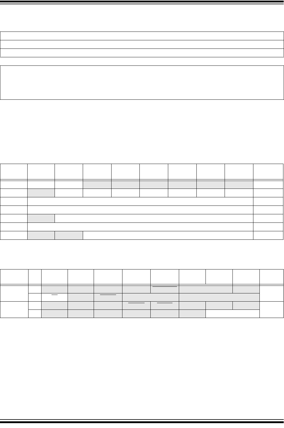
TABLE 10-3: SUMMARY OF REGISTERS ASSOCIATED WITH FLASH PROGRAM MEMORY
TABLE 10-4: SUMMARY OF CONFIGURATION WORD WITH FLASH PROGRAM MEMORY
REGISTER 10-6: PMCON2: PROGRAM MEMORY CONTROL 2 REGISTER
W-0/0 W-0/0 W-0/0 W-0/0 W-0/0 W-0/0 W-0/0 W-0/0
Program Memory Control Register 2
bit 7 bit 0
Legend:
R = Readable bit W = Writable bit U = Unimplemented bit, read as ‘0’
S = Bit can only be set x = Bit is unknown -n/n = Value at POR and BOR/Value at all other Resets
‘1’ = Bit is set ‘0’ = Bit is cleared
bit 7-0 Flash Memory Unlock Pattern bits
To unlock writes, a 55h must be written first, followed by an AAh, before setting the WR bit of the
PMCON1 register. The value written to this register is used to unlock the writes. There are specific
timing requirements on these writes.
Name Bit 7 Bit 6 Bit 5 Bit 4 Bit 3 Bit 2 Bit 1 Bit 0
Register on
Page
INTCON GIE PEIE
TMR0IE INTE IOCIE TMR0IF INTF IOCIF
76
PMCON1
—
(1)
CFGS LWLO FREE WRERR WREN WR RD
107
PMCON2 Program Memory Control Register 2
108
PMADRL PMADRL<7:0>
106
PMADRH
—
(1)
PMADRH<6:0> 106
PMDATL PMDATL<7:0>
106
PMDATH
— —PMDATH<5:0>106
Legend: — = unimplemented location, read as ‘0’. Shaded cells are not used by Flash program memory.
Note 1: Unimplemented, read as ‘1’.
Name Bits Bit -/7 Bit -/6 Bit 13/5 Bit 12/4 Bit 11/3 Bit 10/2 Bit 9/1 Bit 8/0
Register
on Page
CONFIG1
13:8
— —
FCMEN IESO
CLKOUTEN BOREN<1:0> —
42
7:0 CP MCLRE PWRTE WDTE<1:0> FOSC<2:0>
CONFIG2
13:8
— — LVP DEBUG LPBOR BORV STVREN —
44
7:0 — — — — — —WRT<1:0>
Legend: — = unimplemented location, read as ‘0’. Shaded cells are not used by Flash program memory.