
Information

PIC16(L)F1454/1455/1459
DS80000546E-page 4 2012-2013 Microchip Technology Inc.
Data Sheet Clarifications
The following typographic corrections and clarifications
are to be noted for the latest version of the device data
sheet (DS41639A):
1. Module: Electrical Specifications
29.9 AC Characteristics
Removed “No missing codes” from AD03
Conditions column, and modified Note 2. Under
very rare circumstances, a single code can be
missed.
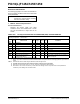
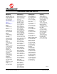
TABLE 29-6: PIC16(L)F1454/1455/1459 A/D CONVERTER (ADC) CHARACTERISTICS
Note: Corrections are shown in bold. Where
possible, the original bold text formatting
has been removed for clarity.
Standard Operating Conditions (unless otherwise stated)
Operating temperature Tested at 25°C
Param
No.
Sym. Characteristic Min. Typ† Max. Units Conditions
AD01 N
R Resolution — — 10 bit
AD02 E
IL Integral Error — — ±1.7 LSb VREF = 3.0V
AD03 E
DL Differential Error — — ±1 LSb VREF = 3.0V
AD04 E
OFF Offset Error — — ±2.5 LSb VREF = 3.0V
AD05 E
GN Gain Error — — ±2.0 LSb VREF = 3.0V
AD06 V
REF Reference Voltage
(3)
1.8 — VDD VVREF = (VREF+ minus VREF-)
AD07 V
AIN Full-Scale Range VSS —VREF V
AD08 Z
AIN Recommended Impedance of
Analog Voltage Source
—— 10k Can go higher if external 0.01F capacitor is
present on input pin.
* These parameters are characterized but not tested.
† Data in “Typ” column is at 3.0V, 25°C unless otherwise stated. These parameters are for design guidance only and are not
tested.
Note 1: Total Absolute Error includes integral, differential, offset and gain errors.
2: The A/D conversion result never decreases with an increase in the input voltage.
3: ADC V
REF is from external VREF+ pin, VDD pin, whichever is selected as reference input.
4: When ADC is off, it will not consume any current other than leakage current. The power-down current specification
includes any such leakage from the ADC module.