
Information


DS80011C-page 8
1999 Microchip Technology Inc.
PIC16C773
The typical Vref line regulation should be the value spec-
ified in Table 15-2 below.
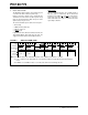
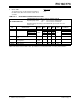
TABLE 15-2 ELECTRICAL CHARACTERISTICS: VREF
DC CHARACTERISTICS
Standard Operating Conditions (unless otherwise stated)
Operating temperature -40°C ≤ T
A ≤ +85°C for industrial and
0°C ≤ T
A ≤ +70°C for commercial
Operating voltage V
DD range as described in DC spec Section 15.1 and Section 15.2.
Param
No.
Characteristic Symbol Min Typ† Max Units Conditions
D400
Output Voltage VRL 2.0 2.048 2.1 V V
DD ≥ 2.5V
VRH 4.0 4.096 4.2 V V
DD ≥ 4.5V
D401A VRL Quiescent Supply Current ∆IV
RL
—
70 TBD µA No load on VRL.
D401B VRH Quiescent Supply Current ∆IV
RH
—
70 TBD µA No load on VRH.
D402 Ouput Voltage Drift TCV
OUT
—
15* 50* ppm/°C Note 1
D404 External Load Source I
VREFSO
——
5* mA
D405 External Load Sink I
VREFSI
——
-5* mA
D406 Load Regulation
∆VOUT/
∆I
OUT
—
1TBD*
mV/mA
Isource = 0 mA to
5mA
—
1 TBD* Isink = 0 mA to
5mA
D407 Line Regulation
∆V
OUT/
∆V
DD
— 1
—
mV/V
* These parameters are characterized but not tested.
† Data in “Typ” column is at 5V, 25°C unless otherwise stated. These parameters are for design guidance
only and are not tested.
Note 1: Production tested at TAMB = 25°C. Specifications over temp limits ensured by characterization.