
Information


2001 Microchip Technology Inc. DS80061C-page 11
PIC16C773
8. The A/D clock source bits (ADCS1:ADCS0)
have had their operation modified. See
Register 1 for a new definition of the ADCS1 and
ADCS0 bits.
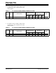
Figure 1 shows how the T
AD time is determined
based upon the selection of the ADCS<1:0> bits
and the source of V
REF+ and VREF-. When VREF+
or V
REF- comes from the internal voltage refer-
ence (VRH or VRL), then the required T
AD time is
increased by a factor of eight (see electrical spec-
ification parameter #130A).
The clock source selected by the ADCS<1:0> bits
is divided by eight when an internally generated
reference voltage is used as reference to the A/D
module. This automatically addresses the require-
ment for the T
AD time when the internal voltage ref-
erence is used as the A/D voltage reference.
FIGURE 1: A/D CLOCK SOURCE
BLOCK DIAGRAM
Table 7 shows the maximum device frequency
depending on the A/D clock source selected.
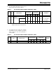
REGISTER 1: A/D CONTROL REGISTER 0 (ADCON0)
Note: Electrical specification parameter #130A is
currently specified in clarifications and cor-
rections section of the Device Errata Sheet.
00
1
0
T
AD
÷8
A/D
Converter
FOSC/2
F
OSC/8
F
OSC/32
A/D RC
Oscillator
01
10
11
V
REF+ = VRH
V
REF+ = VRL
V
REF- = VRL
ADCS<1:0>
R/W-0 R/W-0 R/W-0 R/W-0 R/W-0 R/W-0 R/W-0 R/W-0
ADCS1 ADCS0 CHS2 CHS1 CHS0 GO/DONE
CHS3 ADON
bit 7 bit 0
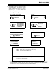
bit 7-6 ADCS<1:0>: A/D Conversion Clock Select bits:
bit 5-0 No change to the operation of these bits
Legend:
R = Readable bit W = Writable bit U = Unimplemented bit, read as ‘0’
- n = Value at POR ’1’ = Bit is set ’0’ = Bit is cleared x = Bit is unknown
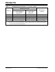
ADCS<1:0>
A/D Clock Source (T
AD) =
When VCFG<2:0> = 000, 001,
011 or 101
When VCFG<2:0> = 010, 100,
110 or 111
00 2 TOSC 16 TOSC
01 8 TOSC 64 TOSC
10 32 TOSC 256 TOSC
11
A/D RC
(1 MHz max)
A/D RC
(125 KHz max)