
Datasheet


PIC16C7X
DS30390E-page 234 1997 Microchip Technology Inc.
Applicable Devices 72 73 73A 74 74A 76 77
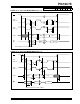
TABLE 20-8: SPI MODE REQUIREMENTS
Parameter
No.
Sym Characteristic Min Typ† Max Units Conditions
70* TssL2scH,
TssL2scL
SS↓ to SCK↓ or SCK↑ input TCY ——ns
71* TscH SCK input high time (slave mode) TCY + 20 — — ns
72* TscL SCK input low time (slave mode) TCY + 20 — — ns
73* TdiV2scH,
TdiV2scL
Setup time of SDI data input to SCK
edge
100 — — ns
74* TscH2diL,
TscL2diL
Hold time of SDI data input to SCK
edge
100 — — ns
75* TdoR SDO data output rise time — 10 25 ns
76* TdoF SDO data output fall time — 10 25 ns
77* TssH2doZ SS↑ to SDO output hi-impedance 10 — 50 ns
78* TscR SCK output rise time (master mode) — 10 25 ns
79* TscF SCK output fall time (master mode) — 10 25 ns
80* TscH2doV,
TscL2doV
SDO data output valid after SCK
edge
— — 50 ns
81* TdoV2scH,
TdoV2scL
SDO data output setup to SCK
edge
TCY ——ns
82* TssL2doV SDO data output valid after SS↓
edge
— — 50 ns
83* TscH2ssH,
TscL2ssH
SS ↑ after SCK edge 1.5TCY + 40 — — ns
* These parameters are characterized but not tested.
† Data in "Typ" column is at 5V, 25˚C unless otherwise stated. These parameters are for design guidance only and are not
tested.