
Datasheet


PIC16C7X
DS30390E-page 216 1997 Microchip Technology Inc.
Applicable Devices 72 73 73A 74 74A 76 77
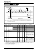
FIGURE 19-12: USART SYNCHRONOUS TRANSMISSION (MASTER/SLAVE) TIMING
TABLE 19-11: USART SYNCHRONOUS TRANSMISSION REQUIREMENTS
FIGURE 19-13: USART SYNCHRONOUS RECEIVE (MASTER/SLAVE) TIMING
TABLE 19-12: USART SYNCHRONOUS RECEIVE REQUIREMENTS
Param
No.
Sym Characteristic Min Typ† Max Units Conditions
120 TckH2dtV SYNC XMIT (MASTER &
SLAVE)
Clock high to data out valid
PIC16C73A/74A — — 80 ns
PIC16LC73A/74A — — 100 ns
121 Tckrf Clock out rise time and fall time
(Master Mode)
PIC16C73A/74A — — 45 ns
PIC16LC73A/74A — — 50 ns
122 Tdtrf Data out rise time and fall time PIC16C73A/74A — — 45 ns
PIC16LC73A/74A — — 50 ns
†: Data in “Typ” column is at 5V, 25°C unless otherwise stated. These parameters are for design guidance only and are not
tested.
Parameter
No.
Sym Characteristic Min Typ† Max Units Conditions
125 TdtV2ckL SYNC RCV (MASTER & SLA
VE)
Data setup before CK ↓ (DT setup time) 15 — — ns
126 TckL2dtl Data hold after CK ↓ (DT hold time) 15 — — ns
†: Data in “Typ” column is at 5V, 25°C unless otherwise stated. These parameters are for design guidance only and are not
tested.
Note: Refer to Figure 19-1 for load conditions
121
121
122
RC6/TX/CK
RC7/RX/DT
pin
pin
120
Note: Refer to Figure 19-1 for load conditions
125
126
RC6/TX/CK
RC7/RX/DT
pin
pin