
Datasheet


1997 Microchip Technology Inc. DS30390E-page 125
PIC16C7X
13.8 Use of the CCP Trigger
An A/D conversion can be started by the “special event
trigger” of the CCP2 module (CCP1 on the PIC16C72
only). This requires that the CCP2M3:CCP2M0 bits
(CCP2CON<3:0>) be programmed as 1011 and that
the A/D module is enabled (ADON bit is set). When the
trigger occurs, the GO/DONE
bit will be set, starting the
A/D conversion, and the Timer1 counter will be reset to
zero. Timer1 is reset to automatically repeat the A/D
acquisition period with minimal software overhead
(moving the ADRES to the desired location). The
appropriate analog input channel must be selected and
the minimum acquisition done before the “special event
trigger” sets the GO/DONE
bit (starts a conversion).
If the A/D module is not enabled (ADON is cleared),
then the “special event trigger” will be ignored by the
A/D module, but will still reset the Timer1 counter.
13.9 Connection Considerations
If the input voltage exceeds the rail values (VSS or VDD)
by greater than 0.2V, then the accuracy of the conver-
sion is out of specification.
An external RC filter is sometimes added for anti-alias-
ing of the input signal. The R component should be
selected to ensure that the total source impedance is
kept under the 10 kΩ recommended specification. Any
external components connected (via hi-impedance) to
an analog input pin (capacitor, zener diode, etc.) should
have very little leakage current at the pin.
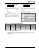
13.10 Transfer Function
The ideal transfer function of the A/D converter is as
follows: the first transition occurs when the analog input
voltage (V
AIN) is Analog VREF/256 (Figure 13-5).
Applicable Devices
72
73 73A 74 74A 76 77
Note: In the PIC16C72, the "special event trig-
ger" is implemented in the CCP1 module.
Applicable Devices
72
73 73A 74 74A 76 77
Applicable Devices
72
73 73A 74 74A 76 77
FIGURE 13-5: A/D TRANSFER FUNCTION
13.11 Ref
erences
A very good reference for understanding A/D convert-
ers is the "Analog-Digital Conversion Handbook" third
edition, published by Prentice Hall (ISBN
0-13-03-2848-0).
Digital code output
FFh
FEh
04h
03h
02h
01h
00h
0.5 LSb
1 LSb
2 LSb
3 LSb
4 LSb
255 LSb
256 LSb
(full scale)
Analog input voltage