
Datasheet


PIC16C7X
DS30390E-page 108 1997 Microchip Technology Inc.
12.2.2 USART ASYNCHRONOUS RECEIVER
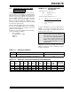
The receiver block diagram is shown in Figure 12-10.
The data is received on the RC7/RX/DT pin and drives
the data recovery block. The data recovery block is
actually a high speed shifter operating at x16 times the
baud rate, whereas the main receive serial shifter oper-
ates at the bit rate or at F
OSC.
Once Asynchronous mode is selected, reception is
enabled by setting bit CREN (RCSTA<4>).
The heart of the receiver is the receive (serial) shift reg-
ister (RSR). After sampling the STOP bit, the received
data in the RSR is transferred to the RCREG register (if
it is empty). If the transfer is complete, flag bit RCIF
(PIR1<5>) is set. The actual interrupt can be enabled/
disabled by setting/clearing enable bit RCIE
(PIE1<5>). Flag bit RCIF is a read only bit which is
cleared by the hardware. It is cleared when the RCREG
register has been read and is empty. The RCREG is a
double buffered register, i.e. it is a two deep FIFO. It is
possible for two bytes of data to be received and trans-
ferred to the RCREG FIFO and a third byte begin shift-
ing to the RSR register. On the detection of the STOP
bit of the third byte, if the RCREG register is still full
then overrun error bit OERR (RCSTA<1>) will be set.
The word in the RSR will be lost. The RCREG register
can be read twice to retrieve the two bytes in the FIFO.
Overrun bit OERR has to be cleared in software. This
is done by resetting the receive logic (CREN is cleared
and then set). If bit OERR is set, transfers from the
RSR register to the RCREG register are inhibited, so it
is essential to clear error bit OERR if it is set. Framing
error bit FERR (RCSTA<2>) is set if a stop bit is
detected as clear. Bit FERR and the 9th receive bit are
buffered the same way as the receive data. Reading
the RCREG, will load bits RX9D and FERR with new
values, therefore it is essential for the user to read the
RCSTA register bef
ore reading RCREG register in
order not to lose the old FERR and RX9D information.
FIGURE 12-10: USART RECEIVE BLOCK DIAGRAM
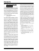
FIGURE 12-11: ASYNCHRONOUS RECEPTION
x64 Baud Rate CLK
SPBRG
Baud Rate Generator
RC7/RX/DT
Pin Buffer
and Control
SPEN
Data
Recovery
CREN
OERR
FERR
RSR register
MSb
LSb
RX9D
RCREG register
FIFO
Interrupt
RCIF
RCIE
Data Bus
8
÷ 64
÷ 16
or
Stop
Start
(8)
7
1
0
RX9
• • •
Start
bit
bit7/8
bit1bit0
bit7/8 bit0Stop
bit
Start
bit
Start
bit
bit7/8
Stop
bit
RX (pin)
reg
Rcv buffer reg
Rcv shift
Read Rcv
buffer reg
RCREG
RCIF
(interrupt flag)
OERR bit
CREN
WORD 1
RCREG
WORD 2
RCREG
Stop
bit
Note: This timing diagram shows three words appearing on the RX input. The RCREG (receive buffer) is read after the third word,
causing the OERR (overrun) bit to be set.