
Information

PIC16C712/716
DS80072D-page 6 2003 Microchip Technology Inc.
Clarifications/Corrections to the Data
Sheet:
In the Device Data Sheet (DS41106A), the following
clarifications and corrections should be noted.
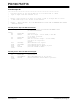
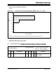
1. The following register and bit names need the
following corrections:
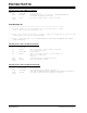
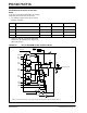
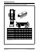
2. Figure 3-4, page 24, of the Device Data Sheet
should show the following block diagram for
RB1/T1OSO/T1CK1:
FIGURE 3-4: BLOCK DIAGRAM OF RB1/T1OSO/T1CKI PIN
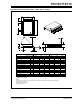
Page Where Occurrence Data Sheet Name Correct Name
10 Figure 2-3, Address 0Fh 1 TRM1H TMR1H
10 Figure 2-3, Address 11h 1 TRM2 TMR2
41 Table 7-2, Address 07h, bit 0 1 TT1CK DT1CK
44 Table 7-5, Control Bits column 4 TR1SCCP TRISCCP
0
1
QD
Q
CK
QD
Q
CK
QD
Q
CK
QD
Q
CK
0
1
0
1
TTL Buffer
TRISB<1>
PORTB<1>
TRISCCP<0>
DATACCP<0>
RB1/T1OSO/T1CKI
RD
Data Bus
WR
WR
WR
WR TRISB
T1OSCEN
RD PORTB
TMR1CS
DATACCP
DATACCP
TRISCCP
PORTB
T1CLKIN
ST
Buffer
P
V
DD
Weak
Pull-up
RBPU
(1)
T1OSCEN
T1CS
VSS
VDD
Note 1: To enable weak pull-ups, set the appropriate TRIS bit(s) and clear the RBPU bit (OPTION_REG<7>).
0
1
TMR1CS