
Information

PIC16C715
DS80082C-page 2 2003 Microchip Technology Inc.
Clarifications/Corrections to the Data
Sheet:
In the Device Data Sheet (DS30272A), the following
clarifications and corrections should be noted.
1. Module: Core (DC Characteristics)
Section 13.3 has changed as shown below.
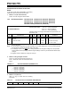
13.3 DC Characteristics: PIC16C715-04 (Commercial, Industrial, Extended)
PIC16C715-10 (Commercial, Industrial, Extended)
PIC16C715-20 (Commercial, Industrial, Extended)
PIC16LC715-04 (Commercial, Industrial)
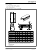
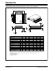
2. Module: Analog-to-Digital Converter
Figure 7-2, page 38, should change from bit 6-3 to
bit 4-3, which will include the information listed
below:
FIGURE 7-2: ADCON0 REGISTER (ADDRESS 1Fh)
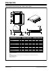
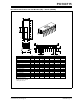
3. Module: Core (Pinouts)
Table 3-1, page 9, should show the following
information:
Table 3-1: PIC16C710/71/711/715 PINOUT DESCRIPTION
DC CHARACTERISTICS
Standard Operating Conditions (unless otherwise stated)
Operating temperature 0°C ≤ T
A ≤ +70°C (commercial)
-40°C ≤ T
A ≤ +85°C (industrial)
-40°C ≤ T
A ≤ +125°C (extended)
Operating voltage V
DD range as described in DC spec Section 13.1
and Section 13.2.
Param
No.
Characteristic Sym Min Typ† Max Units Conditions
Input Low Voltage
I/O ports: VIL
D030 with TTL buffer Vss — 0.15VDD V For entire VDD range
D031 Vss — 0.8V V 4.5 ≤ V
DD ≤ 5.5V
† Data in “Typ” column is at 5V, 25°C unless otherwise stated. These parameters are for design guidance only
and are not tested.
Note 1: In RC oscillator configuration, the OSC1/CLKIN pin is a Schmitt Trigger input. It is not recommended that
the PIC16C7X be driven with external clock in RC mode.
2: The leakage current on the MCLR
pin is strongly dependent on the applied voltage level. The specified
levels represent normal operating conditions. Higher leakage current may be measured at different input
voltages.
3: Negative current is defined as coming out of the pin.
bit 4-3: CHS1:CHS0: Analog Channel Select bits
00 = channel 0, (RA0/AN0)
01 = channel 1, (RA1/AN1)
10 = channel 2, (RA2/AN2)
11 = channel 3, (RA3/AN3)
Vss 5 5, 6 5 P — Ground reference for logic and I/O pins.