PIC16C715 PIC16C715 Data Sheet Errata The PIC16C715 parts you have received conform functionally to the Device Data Sheet (DS30272A), except for the anomalies described below. None. 2003 Microchip Technology Inc.
PIC16C715 Clarifications/Corrections to the Data Sheet: In the Device Data Sheet (DS30272A), the following clarifications and corrections should be noted. 1. Module: Core (DC Characteristics) Section 13.3 has changed as shown below. 13.
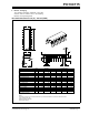
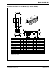
PIC16C715 4. Module: Packaging The package information contained in the data sheet is incorrect. Please refer to the following tables for correct package data. 18-Lead Plastic Dual In-line (P) – 300 mil (PDIP) E1 D 2 n α 1 E A2 A L c A1 B1 β p B eB Units Dimension Limits n p MIN INCHES* NOM 18 .100 .155 .130 MAX MILLIMETERS NOM 18 2.54 3.56 3.94 2.92 3.30 0.38 7.62 7.94 6.10 6.35 22.61 22.80 3.18 3.30 0.20 0.29 1.14 1.46 0.36 0.46 7.87 9.
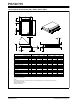
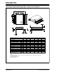
PIC16C715 18-Lead Plastic Small Outline (SO) – Wide, 300 mil (SOIC) E p E1 D 2 B n 1 h α 45° c A2 A φ β L Units Dimension Limits n p Number of Pins Pitch Overall Height Molded Package Thickness Standoff § Overall Width Molded Package Width Overall Length Chamfer Distance Foot Length Foot Angle Lead Thickness Lead Width Mold Draft Angle Top Mold Draft Angle Bottom A A2 A1 E E1 D h L φ c B α β MIN .093 .088 .004 .394 .291 .446 .010 .016 0 .009 .014 0 0 A1 INCHES* NOM 18 .050 .099 .091 .
PIC16C715 18-Lead Ceramic Dual In-line with Window (JW) – 300 mil (CERDIP) E1 D W2 2 n 1 W1 E A2 A c L A1 eB B1 p B Units Dimension Limits n p Number of Pins Pitch Top to Seating Plane Ceramic Package Height Standoff Shoulder to Shoulder Width Ceramic Pkg. Width Overall Length Tip to Seating Plane Lead Thickness Upper Lead Width Lower Lead Width Overall Row Spacing § Window Width Window Length * Controlling Parameter § Significant Characteristic JEDEC Equivalent: MO-036 Drawing No.
PIC16C715 20-Lead Plastic Shrink Small Outline (SS) – 209 mil, 5.30 mm (SSOP) E E1 p D B 2 1 n α c A2 A φ L A1 β Units Dimension Limits n p Number of Pins Pitch Overall Height Molded Package Thickness Standoff § Overall Width Molded Package Width Overall Length Foot Length Lead Thickness Foot Angle Lead Width Mold Draft Angle Top Mold Draft Angle Bottom A A2 A1 E E1 D L c φ B α β MIN .068 .064 .002 .299 .201 .278 .022 .004 0 .010 0 0 INCHES* NOM 20 .026 .073 .068 .006 .309 .207 .284 .030 .
PIC16C715 APPENDIX A: REVISION HISTORY Rev. A Document 9/2000 First revision of this document. Rev. B Document 6/2001 Under Clarifications/Corrections to the Data Sheet, added issue 2 (Analog-to-Digital Converter) and issue 3 (Core). Rev. C Document 3/2003 Under Clarifications/Corrections to the Data Sheet, Item 4, Packaging: correct package data was added. 2003 Microchip Technology Inc.
PIC16C715 NOTES: DS80082C-page 8 2003 Microchip Technology Inc.
Note the following details of the code protection feature on Microchip devices: • Microchip products meet the specification contained in their particular Microchip Data Sheet. • Microchip believes that its family of products is one of the most secure families of its kind on the market today, when used in the intended manner and under normal conditions. • There are dishonest and possibly illegal methods used to breach the code protection feature.
WORLDWIDE SALES AND SERVICE AMERICAS ASIA/PACIFIC Japan Corporate Office Australia 2355 West Chandler Blvd. Chandler, AZ 85224-6199 Tel: 480-792-7200 Fax: 480-792-7277 Technical Support: 480-792-7627 Web Address: http://www.microchip.com Microchip Technology Australia Pty Ltd Marketing Support Division Suite 22, 41 Rawson Street Epping 2121, NSW Australia Tel: 61-2-9868-6733 Fax: 61-2-9868-6755 Microchip Technology Japan K.K.