
Datasheet


1997-2013 Microchip Technology Inc. DS30234E-page 71
PIC16C6X
8.0 TIMER1 MODULE
Timer1 is a 16-bit timer/counter consisting of two 8-bit
registers (TMR1H and TMR1L) which are readable and
writable. Register TMR1 (TMR1H:TMR1L) increments
from 0000h to FFFFh and rolls over to 0000h. The
TMR1 Interrupt, if enabled, is generated on overflow
which is latched in interrupt flag bit TMR1IF (PIR1<0>).
This interrupt can be enabled/disabled by setting/clear-
ing the TMR1 interrupt enable bit TMR1IE (PIE1<0>).
Timer1 can operate in one of two modes:
•As a timer
• As a counter
The operating mode is determined by clock select bit,
TMR1CS (T1CON<1>) (Figure 8-2).
In timer mode, Timer1 increments every instruction
cycle. In counter mode, it increments on every rising
edge of the external clock input.
Timer1 can be enabled/disabled by setting/clearing
control bit TMR1ON (T1CON<0>).
Applicable Devices
61 62 62A R62 63 R63 64 64A R64 65 65A R65 66 67
Timer1 also has an internal “reset input”. This reset can
be generated by CCP1 or CCP2 (Capture/Compare/
PWM) module. See Section 10.0 for details. Figure 8-1
shows the Timer1 control register.
For the PIC16C62A/R62/63/R63/64A/R64/65A/R65/
R66/67, when the Timer1 oscillator is enabled
(T1OSCEN is set), the RC1 and RC0 pins become
inputs. That is, the TRISC<1:0> value is ignored.
For the PIC16C62/64/65, when the Timer1 oscillator is
enabled (T1OSCEN is set), RC1 pin becomes an input,
however the RC0 pin will have to be configured as an
input by setting the TRISC<0> bit.
The Timer1 module also has a software programmable
prescaler.
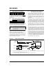
FIGURE 8-1: T1CON: TIMER1 CONTROL REGISTER (ADDRESS 10h)
U-0 U-0 R/W-0 R/W-0 R/W-0 R/W-0 R/W-0 R/W-0
— — T1CKPS1 T1CKPS0 T1OSCEN T1SYNC TMR1CS TMR1ON R = Readable bit
W = Writable bit
U = Unimplemented bit,
read as ‘0’
- n = Value at POR reset
bit7 bit0
bit 7-6: Unimplemented: Read as '0'
bit 5-4: T1CKPS1:T1CKPS0: Timer1 Input Clock Prescale Select bits
11 = 1:8 Prescale value
10 = 1:4 Prescale value
01 = 1:2 Prescale value
00 = 1:1 Prescale value
bit 3: T1OSCEN: Timer1 Oscillator Enable Control bit
1 = Oscillator is enabled
0 = Oscillator is shut off
Note: The oscillator inverter and feedback resistor are turned off to eliminate power drain.
bit 2: T1S
YNC: Timer1 External Clock Input Synchronization Control bit
TMR1CS = 1
1 = Do not synchronize external clock input
0 = Synchronize external clock input
TMR1CS = 0
This bit is ignored. Timer1 uses the internal clock when TMR1CS = 0.
bit 1: TMR1CS: Timer1 Clock Source Select bit
1 = External clock from T1OSI (on the rising edge) (See pinouts for pin with T1OSI function)
0 = Internal clock (Fosc/4)
bit 0: TMR1ON: Timer1 On bit
1 = Enables Timer1
0 = Stops Timer1