
Datasheet


PIC16C6X
DS30234E-page 58 1997-2013 Microchip Technology Inc.
5.5 PORTE and TRISE Register
PORTE has three pins, RE2/CS, RE1/WR, and
RE0/RD
which are individually configurable as inputs
or outputs. These pins have Schmitt Trigger input buf-
fers.
I/O PORTE becomes control inputs for the micropro-
cessor port when bit PSPMODE (TRISE<4>) is set. In
this mode, the user must make sure that the
TRISE<2:0> bits are set (pins are configured as digital
inputs). In this mode the input buffers are TTL.
Figure 5-9 shows the TRISE register, which controls
the parallel slave port operation and also controls the
direction of the PORTE pins.
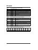
Applicable Devices
61 62 62A R62 63 R636464AR646565AR6566 67
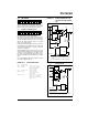
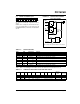
FIGURE 5-8: PORTE BLOCK DIAGRAM
(IN I/O PORT MODE)
Data
bus
WR
PORT
WR
TRIS
RD PORT
Data Latch
TRIS Latch
RD TRIS
Schmitt
Tr ig ger
input
buffer
QD
CK
QD
CK
EN
QD
EN
I/O pin
(1)
Note 1: I/O pins have protection diodes to VDD and VSS.
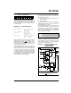
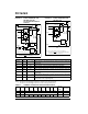
FIGURE 5-9: TRISE REGISTER (ADDRESS 89h)
R-0 R-0 R/W-0 R/W-0 U-0 R/W-1 R/W-1 R/W-1
IBF OBF IBOV PSPMODE
— bit2 bit1 bit0 R = Readable bit
W = Writable bit
U = Unimplemented bit,
read as ‘0’
- n = Value at POR reset
bit7 bit0
bit 7 : IBF: Input Buffer Full Status bit
1 = A word has been received and is waiting to be read by the CPU
0 = No word has been received
bit 6: OBF: Output Buffer Full Status bit
1 = The output buffer still holds a previously written word
0 = The output buffer has been read
bit 5: IBOV: Input Buffer Overflow Detect bit (in microprocessor mode)
1 = A write occurred when a previously input word has not been read (must be cleared in software)
0 = No overflow occurred
bit 4: PSPMODE: Parallel Slave Port Mode Select bit
1 = Parallel slave port mode
0 = General purpose I/O mode
bit 3: Unimplemented: Read as '0'
PORTE Data Direction Bits
bit 2: Bit2: Direction Control bit for pin RE2/CS
1 = Input
0 = Output
bit 1: Bit1: Direction Control bit for pin RE1/WR
1 = Input
0 = Output
bit 0: Bit0: Direction Control bit for pin RE0/RD
1 = Input
0 = Output