
Datasheet


PIC16C6X
DS30234E-page 212 1997-2013 Microchip Technology Inc.
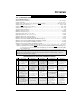
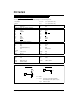
Applicable Devices 61 62 62A R62 63 R63 64 64A R64 65 65A R65 66 67
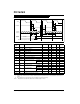
19.1 DC Characteristics: PIC16C65-04 (Commercial, Industrial)
PIC16C65-10 (Commercial, Industrial)
PIC16C65-20 (Commercial, Industrial)
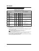
DC CHARACTERISTICS
Standard Operating Conditions (unless otherwise stated)
Operating temperature -40°C T
A +85°C for industrial and
0°C T
A +70°C for commercial
Param
No.
Characteristic Sym Min Typ† Max Units Conditions
D001
D001A
Supply Voltage V
DD 4.0
4.5
-
-
6.0
5.5
V
V
XT, RC and LP osc configuration
HS osc configuration
D002* RAM Data Retention
Voltage (Note 1)
V
DR -1.5- V
D003 V
DD start voltage to
ensure internal Power-on
Reset signal
VPOR -VSS - V See section on Power-on Reset for details
D004* V
DD rise rate to ensure
internal Power-on Reset
signal
SVDD 0.05 - - V/ms See section on Power-on Reset for details
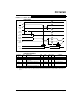
D010
D013
Supply Current (Note 2, 5) I
DD -
-
2.7
13.5
5
30
mA
mA
XT, RC osc configuration
F
OSC = 4 MHz, VDD = 5.5V (Note 4)
HS osc configuration
F
OSC = 20 MHz, VDD = 5.5V
D020
D021
D021A
Power-down Current
(Note 3, 5)
I
PD -
-
-
10.5
1.5
1.5
800
800
800
A
A
A
VDD = 4.0V, WDT enabled,-40C to +85C
V
DD = 4.0V, WDT disabled,-0C to +70C
V
DD = 4.0V, WDT disabled,-40C to +85C
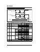
* These parameters are characterized but not tested.
† Data in "Typ" column is at 5V, 25°C unless otherwise stated. These parameters are for design guidance only
and are not tested.
Note 1: This is the limit to which V
DD can be lowered without losing RAM data.
2: The supply current is mainly a function of the operating voltage and frequency. Other factors such as I/O pin
loading and switching rate, oscillator type, internal code execution pattern, and temperature also have an
impact on the current consumption.
The test conditions for all I
DD measurements in active operation mode are:
OSC1 = external square wave, from rail to rail; all I/O pins tristated, pulled to V
DD,
MCLR
= VDD; WDT enabled/disabled as specified.
3: The power down current in SLEEP mode does not depend on the oscillator type. Power-down current is mea-
sured with the part in SLEEP mode, with all I/O pins in hi-impedance state and tied to V
DD and VSS.
4: For RC osc configuration, current through Rext is not included. The current through the resistor can be esti-
mated by the formula Ir = V
DD/2Rext (mA) with Rext in kOhm.
5: Timer1 oscillator (when enabled) adds approximately 20 A to the specification. This value is from character-
ization and is for design guidance only. This is not tested.