
Datasheet


1997-2013 Microchip Technology Inc. DS30234E-page 163
PIC16C6X
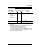
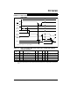
Applicable Devices 61 62 62A R62 63 R63 64 64A R64 65 65A R65 66 67
Output High Voltage
D090 I/O ports (Note 3) V
OH VDD-0.7 - - V IOH = -3.0 mA,
V
DD = 4.5V, -40C to +85C
D090A V
DD-0.7 - - V IOH = -2.5 mA,
V
DD = 4.5V, -40C to +125C
D092 OSC2/CLKOUT (RC osc config) V
DD-0.7 - - V IOH = -1.3 mA,
V
DD = 4.5V, -40C to +85C
D092A V
DD-0.7 - - V IOH = -1.0 mA,
V
DD = 4.5V, -40C to +125C
D150* Open-Drain High Voltage V
OD - - 14 V RA4 pin
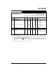
Capacitive Loading Specs on
Output Pins
D100 OSC2 pin C
OSC2 15 pF In XT, HS and LP modes when
external clock is used to drive
OSC1.
D101 All I/O pins and OSC2 (in RC mode) C
IO 50 pF
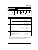
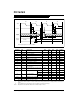
DC CHARACTERISTICS
Standard Operating Conditions (unless otherwise stated)
Operating temperature -40°C T
A +125°C for extended,
-40°C T
A +85°C for industrial and
0°C T
A +70°C for commercial
Operating voltage V
DD range as described in DC spec Section 15.1 and
Section 15.2.
Param
No.
Characteristic Sym Min Typ† Max Units Conditions
* The parameters are characterized but not tested.
† Data in “Typ” column is at 5V, 25C unless otherwise stated. These parameters are for design guidance only
and are not tested.
Note 1: In RC oscillator configuration, the OSC1/CLKIN pin is a Schmitt Trigger input. It is not recommended that the
PIC16C6X be driven with external clock in RC mode.
2: The leakage current on the MCLR
/VPP pin is strongly dependent on the applied voltage level. The specified
levels represent normal operating conditions. Higher leakage current may be measured at different input volt-
ages.
3: Negative current is defined as current sourced by the pin.