
Datasheet


PIC16C6X
DS30234E-page 16 1997-2013 Microchip Technology Inc.
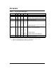
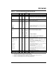
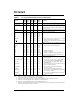
TABLE 3-3: PIC16C64/64A/R64/65/65A/R65/67 PINOUT DESCRIPTION
Pin Name
DIP
Pin#
PLCC
Pin#
TQFP
MQFP
Pin#
Pin
Type
Buffer
Type
Description
OSC1/CLKIN 13 14 30 I
ST/CMOS
(3)
Oscillator crystal input/external clock source input.
OSC2/CLKOUT 14 15 31 O — Oscillator crystal output. Connects to crystal or resonator in
crystal oscillator mode. In RC mode, the pin outputs CLK-
OUT which has 1/4 the frequency of OSC1, and denotes the
instruction cycle rate.
MCLR
/VPP
1 2 18 I/P ST Master clear reset input or programming voltage input. This
pin is an active low reset to the device.
PORTA is a bi-directional I/O port.
RA0 2 3 19 I/O TTL
RA1 3 4 20 I/O TTL
RA2 4 5 21 I/O TTL
RA3 5 6 22 I/O TTL
RA4/T0CKI 6 7 23 I/O ST RA4 can also be the clock input to the Timer0
timer/counter. Output is open drain type.
RA5/SS
7 8 24 I/O TTL RA5 can also be the slave select for the synchronous
serial port.
PORTB is a bi-directional I/O port. PORTB can be software
programmed for internal weak pull-up on all inputs.
RB0/INT 33 36 8 I/O TTL/ST
(4)
RB0 can also be the external interrupt pin.
RB1 34 37 9 I/O TTL
RB2 35 38 10 I/O TTL
RB3 36 39 11 I/O TTL
RB4 37 41 14 I/O TTL Interrupt on change pin.
RB5 38 42 15 I/O TTL Interrupt on change pin.
RB6 39 43 16 I/O TTL/ST
(5)
Interrupt on change pin. Serial programming clock.
RB7 40 44 17 I/O TTL/ST
(5)
Interrupt on change pin. Serial programming data.
PORTC is a bi-directional I/O port.
RC0/T1OSO
(1)
/T1CKI 15 16 32 I/O ST RC0 can also be the Timer1 oscillator output
(1)
or
Timer1 clock input.
RC1/T1OSI
(1)
/CCP2
(2)
16 18 35 I/O ST RC1 can also be the Timer1 oscillator input
(1)
or
Capture2 input/Compare2 output/PWM2 output
(2)
.
RC2/CCP1 17 19 36 I/O ST RC2 can also be the Capture1 input/Compare1 out-
put/PWM1 output.
RC3/SCK/SCL 18 20 37 I/O ST RC3 can also be the synchronous serial clock input/out-
put for both SPI and I
2
C modes.
RC4/SDI/SDA 23 25 42 I/O ST RC4 can also be the SPI Data In (SPI mode) or
data I/O (I
2
C mode).
RC5/SDO 24 26 43 I/O ST RC5 can also be the SPI Data Out (SPI mode).
RC6/TX/CK
(2)
25 27 44 I/O ST RC6 can also be the USART Asynchronous Transmit
(2)
or Synchronous Clock
(2)
.
RC7/RX/DT
(2)
26 29 1 I/O ST RC7 can also be the USART Asynchronous Receive
(2)
or Synchronous Data
(2)
.
Legend: I = input O = output I/O = input/output P = power
— = Not used TTL = TTL input ST = Schmitt Trigger input
Note 1: Pin functions T1OSO and T1OSI are reversed on the PIC16C64.
2: CCP2 and the USART are not available on the PIC16C64/64A/R64.
3: This buffer is a Schmitt Trigger input when configured in RC oscillator mode and a CMOS input otherwise.
4: This buffer is a Schmitt Trigger input when configured as the external interrupt.
5: This buffer is a Schmitt Trigger input when used in serial programming mode.
6: This buffer is a Schmitt Trigger input when configured as general purpose I/O and a TTL input when used in the Parallel Slave
Port mode (for interfacing to a microprocessor bus).