
Information

PIC16C66
DS80097A-page 2 2001 Microchip Technology Inc.
Clarifications/Corrections to the Data
Sheet:
In the Device Data Sheet (DS30234D), the following
clarifications and corrections should be noted.
1. Module: I/O Ports
The specification for the High Voltage Open Drain
I/O (parameter D150, the RA4 pin) cannot be met
without possible long term reliability issues on that
I/O pin. If a high voltage drive is required, use an
external transistor that can support the required
voltage. The new value is shown in Table 2.
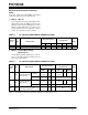
TABLE 2: DC SPECIFICATION CHANGES FROM DATA SHEET
2. Module: SSP (SPI Mode Timing
Specifications)
The SPI interface timings (parameters 71, 71A, 72,
72A, 73, and 73A) have been modified. The new
values are shown in Table 3.
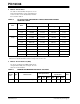
TABLE 3: DC SPECIFICATION CHANGES FROM DATA SHEET
Param
No.
Sym. Characteristic
New Specification
Data Sheet
Specification
Units
Min Typ Max Min Typ Max
D150 V
OD RA4 Open Drain High Voltage — — 10 ——14 V
Param
No.
Sym. Characteristic
New Specification
Data Sheet
Specification
Units
Min Typ Max Min Typ Max
71
T
SCH
SCK input high time
(Slave mode)
Continuous
1.25 T
CY
+ 30 ns
——
T
CY
+ 20 ns
——
ns
71A Single Byte
(1)
40 —— N.A. ns
72
T
SCL
SCK input low time
(Slave mode)
Continuous
1.25 T
CY
+ 30 ns
——
TCY
+ 20 ns
——
ns
72A Single Byte
(1)
40 —— N.A. ns
73A TB2B
Last clock edge of the Byte1 to 1st
clock edge of the Byte2
(1)
1.5 TCY
+ 40 ns
—— N.A.
ns
* This parameter is characterized but not tested.
Note 1: Specification 73A is only required if specifications 71A and 72A are used.