
Datasheet


PIC16C63A/65B/73B/74B
DS30605D-page 96 1998-2013 Microchip Technology Inc.
13.7.2 WDT PROGRAMMING
CONSIDERATIONS
It should also be taken into account that under worst
case conditions (V
DD = Min., Temperature = Max., and
max. WDT prescaler), it may take several seconds
before a WDT time-out occurs.
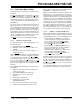
FIGURE 13-6: WATCHDOG TIMER BLOCK DIAGRAM
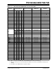
TABLE 13-7: SUMMARY OF WATCHDOG TIMER REGISTERS
Note: When a CLRWDT instruction is executed
and the prescaler is assigned to the WDT,
the prescaler count will be cleared, but the
prescaler assignment is not changed.
From TMR0 Clock Source
(Figure 6-1)
To TMR0 MUX (Figure 6-1)
Postscaler
WDT Timer
WDT
Enable Bit
0
1
M
U
X
PSA
8 - to - 1 MUX
PS2:PS0
0
1
MUX
PSA
WDT
Time-out
Note: PSA and PS2:PS0 are bits in the OPTION register.
8
Address Name Bit 7 Bit 6 Bit 5 Bit 4 Bit 3 Bit 2 Bit 1 Bit 0
2007h Config. bits
–
BODEN
(1)
CP1 CP0
PWRTE
(1)
WDTE FOSC1 FOSC0
81h OPTION_REG
RBPU INTEDG T0CS T0SE PSA PS2 PS1 PS0
Legend: Shaded cells are not used by the Watchdog Timer.
Note 1: See Register 13-1 for operation of these bits.