
Datasheet


PIC16C63A/65B/73B/74B
DS30605D-page 82 1998-2013 Microchip Technology Inc.
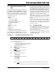
12.1 A/D Acquisition Requirements
For the A/D converter to meet its specified accuracy,
the charge holding capacitor (C
HOLD) must be allowed
to fully charge to the input channel voltage level. The
analog input model is shown in Figure 12-2. The
source impedance (R
S) and the internal sampling
switch (R
SS) impedance directly affect the time
required to charge the capacitor C
HOLD. The sampling
switch (R
SS) impedance varies over the device voltage
(V
DD), Figure 12-2. The source impedance affects the
offset voltage at the analog input (due to pin leakage
current).
The maximum recommended impedance for ana-
log sources is 10 k. After the analog input channel is
selected (changed), the acquisition time (T
ACQ) must
pass before the conversion can be started.
To calculate the minimum acquisition time,
Equation 12-1 may be used. This equation assumes
that 1/2 LSb error is used (512 steps for the A/D). The
1/2 LSb error is the maximum error allowed for the A/D
to meet its specified resolution.
For more information, see the PIC
®
Mid-Range MCU
Family Reference Manual (DS33023). In general, how-
ever, given a maximum source impedance of 10 k
and a worst case temperature of 100°C, T
ACQ will be no
more than 16 sec.
FIGURE 12-2: ANALOG INPUT MODEL
EQUATION 12-1: ACQUISITION TIME
CPIN
VA
Rs
ANx
5 pF
V
DD
VT = 0.6 V
VT = 0.6 V
I leakage
R
IC £ 1k
Sampling
Switch
SS
R
SS
CHOLD
= DAC capacitance
V
SS
6V
Sampling Switch
5V
4V
3V
2V
567891011
(k)
VDD
= 51.2 pF
± 500 nA
Legend: CPIN
VT
I leakage
R
IC
SS
C
HOLD
= input capacitance
= threshold voltage
= leakage current at the pin due to
= interconnect resistance
= sampling switch
= sample/hold capacitance (from DAC)
various junctions
TACQ =
=
Amplifier Settling Time +
Hold Capacitor Charging Time +
Temperature Coefficient
T
AMP + TC + TCOFF
TAMP = 5 S
T
C = - (51.2 pF)(1 k + RSS + RS) In(1/511)
T
COFF = (Temp -25C)(0.05 S/C)