
Datasheet


1998-2013 Microchip Technology Inc. DS30605D-page 81
PIC16C63A/65B/73B/74B
The following steps should be followed for doing an A/D
conversion:
1. Configure the A/D module:
• Configure analog pins, voltage reference,
and digital I/O (ADCON1)
• Select A/D input channel (ADCON0)
• Select A/D conversion clock (ADCON0)
• Turn on A/D module (ADCON0)
2. Configure A/D interrupt (if desired):
• Clear ADIF bit (PIR1<6>)
• Set ADIE bit (PIE1<6>)
• Set PEIE bit (INTCON<6>)
• Set GIE bit (INTCON<7>)
3. Wait the required acquisition time.
4. Set GO/DONE bit (ADCON0) to start conversion.
5. Wait for A/D conversion to complete, by either:
Polling for the GO/DONE
bit to be cleared (if
interrupts are disabled);
OR
Waiting for the A/D interrupt.
6. Read A/D result register (ADRES), clear bit
ADIF if required.
7. For next conversion, go to step 1 or step 2 as
required. The A/D conversion time per bit is
defined as T
AD. A minimum wait of 2 TAD is
required before next acquisition starts.
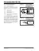
FIGURE 12-1: A/D BLOCK DIAGRAM
(Input Voltage)
V
IN
VREF
(Reference
Voltage)
V
DD
PCFG2:PCFG0
CHS2:CHS0
000 or
010 or
100 or
001 or
011 or
101
RE2/AN7
(1)
RE1/AN6
(1)
RE0/AN5
(1)
RA5/AN4
RA3/AN3/V
REF
RA2/AN2
RA1/AN1
RA0/AN0
111
110
101
100
011
010
001
000
A/D
Converter
Note 1: Not available on PIC16C73B.
11x