
Datasheet


1998-2013 Microchip Technology Inc. DS30605D-page 75
PIC16C63A/65B/73B/74B
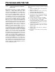
TABLE 11-6: REGISTERS ASSOCIATED WITH SYNCHRONOUS MASTER RECEPTION
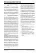
FIGURE 11-8: SYNCHRONOUS RECEPTION (MASTER MODE, SREN)
Address Name Bit 7 Bit 6 Bit 5 Bit 4 Bit 3 Bit 2 Bit 1 Bit 0
Value on:
POR,
BOR
Value on
all other
RESETS
0Bh,8Bh INTCON GIE PEIE
T0IE INTE RBIE T0IF INTF RBIF 0000 000x 0000 000u
0Ch PIR1
PSPIF
(1)
ADIF
(2)
RCIF TXIF SSPIF CCP1IF TMR2IF TMR1IF 0000 0000 0000 0000
18h RCSTA SPEN RX9
SREN CREN — FERR OERR RX9D 0000 -00x 0000 -00x
1Ah RCREG USART Receive register 0000 0000 0000 0000
8Ch PIE1
PSPIE
(1)
ADIE
(2)
RCIE TXIE SSPIE CCP1IE TMR2IE TMR1IE 0000 0000 0000 0000
98h TXSTA CSRC
TX9 TXEN SYNC — BRGH TRMT TX9D 0000 -010 0000 -010
99h SPBRG Baud Rate Generator register 0000 0000 0000 0000
Legend: u = unchanged, x = unknown, - = unimplemented, read as '0'.
Shaded cells are not used for synchronous master reception.
Note 1: Bits PSPIE and PSPIF are reserved on the PIC16C63A/73B; always maintain these bits clear.
2: Bits ADIE and ADIF are reserved on the PIC16C63A/65B; always maintain these bits clear.
CREN bit
RC7/RX/DT pin
RC6/TX/CK pin
Write to
bit SREN
SREN bit
RCIF bit
(interrupt)
Read
RXREG
Note: Timing diagram demonstrates SYNC Master mode with bit SREN = '1' and bit BRG = '0'.
Q3 Q4Q1Q2 Q3Q4Q1 Q2 Q3Q4Q2 Q1 Q2Q3 Q4Q1 Q2 Q3 Q4 Q1Q2Q3 Q4Q1 Q2 Q3Q4 Q1Q2 Q3 Q4Q1Q2 Q3 Q4 Q1 Q2 Q3Q4
'0'
bit0 bit1 bit2 bit3 bit4 bit5 bit6 bit7
'0'
Q1 Q2Q3Q4