
Datasheet


PIC16C63A/65B/73B/74B
DS30605D-page 52 1998-2013 Microchip Technology Inc.
9.2 Compare Mode
In Compare mode, the 16-bit CCPR1 register value is
constantly compared against the TMR1 register pair
value. When a match occurs, the RC2/CCP1 pin is:
• Driven high
•Driven low
• Remains unchanged
The action on the pin is based on the value of control
bits CCP1M3:CCP1M0 (CCP1CON<3:0>). At the
same time, interrupt flag bit CCP1IF is set.
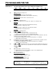
FIGURE 9-2: COMPARE MODE
OPERATION BLOCK
DIAGRAM
9.2.1 CCP PIN CONFIGURATION
The user must configure the RC2/CCP1 pin as an out-
put by clearing the TRISC<2> bit.
9.2.2 TIMER1 MODE SELECTION
Timer1 must be running in Timer mode or Synchro-
nized Counter mode if the CCP module is using the
compare feature. In Asynchronous Counter mode, the
compare operation may not work.
9.2.3 SOFTWARE INTERRUPT MODE
When Generate Software Interrupt mode is chosen, the
CCP1 pin is not affected. The CCPIF bit is set, causing
a CCP interrupt (if enabled).
9.2.4 SPECIAL EVENT TRIGGER
In this mode, an internal hardware trigger is generated,
which may be used to initiate an action.
The special event trigger output of CCP1 resets the
TMR1 register pair. This allows the CCPR1 register to
effectively be a 16-bit programmable period register for
Timer1.
The special event trigger output of CCP2 resets the
TMR1 register pair and starts an A/D conversion (if the
A/D module is enabled).
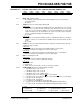
9.3 PWM Mode (PWM)
In Pulse Width Modulation mode, the CCPx pin pro-
duces up to a 10-bit resolution PWM output. Since the
CCP1 pin is multiplexed with the PORTC data latch, the
TRISC<2> bit must be cleared to make the CCP1 pin
an output.
Figure 9-3 shows a simplified block diagram of the
CCP module in PWM mode.
For a step-by-step procedure on how to set up the CCP
module for PWM operation, see Section 9.3.3.
FIGURE 9-3: SIMPLIFIED PWM BLOCK
DIAGRAM
Note: Clearing the CCP1CON register will force
the RC2/CCP1 compare output latch to the
default low level. This is not the PORTC
I/O data latch.
CCPR1H CCPR1L
TMR1H TMR1L
Comparator
QS
R
Output
Logic
Special Event Trigger
Set Flag bit CCP1IF
(PIR1<2>)
Match
RC2/CCP1
TRISC<2>
CCP1CON<3:0>
Mode Select
Output Enable
pin
Special event trigger will:
reset Timer1, but not set interrupt flag bit TMR1IF (PIR1<0>),
and set bit GO/DONE
(ADCON0<2>).
Note: The special event trigger from the
CCP1and CCP2 modules will not set inter-
rupt flag bit TMR1IF (PIR1<0>).
Note: Clearing the CCP1CON register will force
the CCP1 PWM output latch to the default
low level. This is not the PORTC I/O data
latch.
CCPR1L
CCPR1H (Slave)
Comparator
TMR2
Comparator
PR2
(Note 1)
R
Q
S
Duty Cycle Registers
CCP1CON<5:4>
Clear Timer,
CCP1 pin and
latch D.C.
TRISC<2>
RC2/CCP1
Note 1: 8-bit timer is concatenated with 2-bit internal Q clock,
or 2 bits of the prescale, to create 10-bit time-base.