
Datasheet


1998-2013 Microchip Technology Inc. DS30605D-page 37
PIC16C63A/65B/73B/74B
5.6 Parallel Slave Port (PSP)
PORTD operates as an 8-bit wide Parallel Slave Port
(PSP), or microprocessor port when control bit PSP-
MODE (TRISE<4>) is set. In Slave mode, it is asyn-
chronously readable and writable by the external world,
through RD control input pin RE0/RD/AN5 and WR
control input pin RE1/WR/AN6.
It can directly interface to an 8-bit microprocessor data
bus. The external microprocessor can read or write the
PORTD latch as an 8-bit latch. Setting bit PSPMODE
enables port pin RE0/RD
/AN5 to be the RD input,
RE1/WR
/AN6 to be the WR input and RE2/CS/AN7 to
be the CS
(chip select) input. For this functionality, the
corresponding data direction bits of the TRISE register
(TRISE<2:0>) must be configured as inputs (set) and
the A/D port configuration bits PCFG2:PCFG0
(ADCON1<2:0>) must be set, which will configure pins
RE2:RE0 as digital I/O.
There are actually two 8-bit latches, one for data out
(from the PIC
®
MCU) and one for data input. The user
writes 8-bit data to PORTD data latch and reads data
from the port pin latch (note that they have the same
address). In this mode, the TRISD register is ignored
since the external device is controlling the direction of
data flow.
A write to the PSP occurs when both the CS
and WR
lines are first detected low. When either the CS or WR
lines become high (level triggered), then the Input
Buffer Full (IBF) status flag bit (TRISE<7>) is set on the
Q4 clock cycle, following the next Q2 cycle, to signal
the write is complete (Figure 5-9). The interrupt flag bit
PSPIF (PIR1<7>) is also set on the same Q4 clock
cycle. IBF can only be cleared by reading the PORTD
input latch. The Input Buffer Overflow (IBOV) status
flag bit (TRISE<5>) is set if a second write to the PSP
is attempted when the previous byte has not been read
out of the buffer.
A read from the PSP occurs when both the CS
and RD
lines are first detected low. The Output Buffer Full
(OBF) status flag bit (TRISE<6>) is cleared immedi-
ately (Figure 5-10), indicating that the PORTD latch is
waiting to be read by the external bus. When either the
CS
or RD pin becomes high (level triggered), the inter-
rupt flag bit PSPIF is set on the Q4 clock cycle, follow-
ing the next Q2 cycle, indicating that the read is
complete. OBF remains low until data is written to
PORTD by the user firmware.
When not in PSP mode, the IBF and OBF bits are held
clear. However, if flag bit IBOV was previously set, it
must be cleared in firmware.
An interrupt is generated and latched into flag bit
PSPIF when a read or write operation is completed.
PSPIF must be cleared by the user in firmware and the
interrupt can be disabled by clearing the interrupt
enable bit PSPIE (PIE1<7>).
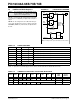
FIGURE 5-8: PORTD AND PORTE
BLOCK DIAGRAM
(PARALLEL SLAVE
PORT)
Note: The PIC16C63A and PIC16C73B do not
provide a parallel slave port. The PORTD,
PORTE, TRISD and TRISE registers are
not implemented.
Data Bus
WR
Port
RD
RDx
QD
CK
EN
QD
EN
Port
pin
One bit of PORTD
Set Interrupt Flag
PSPIF (PIR1<7>)
Read
Chip Select
Write
RD
CS
WR
TTL
TTL
TTL
TTL
Note 1: I/O pins have protection diodes to VDD and VSS.