
Datasheet


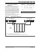


PIC16C63A/65B/73B/74B
DS30605D-page 30 1998-2013 Microchip Technology Inc.
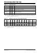
TABLE 5-1: PORTA FUNCTIONS
TABLE 5-2: SUMMARY OF REGISTERS ASSOCIATED WITH PORTA
Name Bit# Buffer Function
RA0/AN0
(1)
bit0 TTL Digital input/output or analog input.
RA1/AN1
(1)
bit1 TTL Digital input/output or analog input.
RA2/AN2
(1)
bit2 TTL Digital input/output or analog input.
RA3/AN3/VREF
(1)
bit3 TTL Digital input/output or analog input or VREF.
RA4/T0CKI bit4 ST
Digital input/output or external clock input for Timer0.
Output is open drain type.
RA5/SS
/AN4
(1)
bit5 TTL Input/output or slave select input for synchronous serial port or analog input.
Legend: TTL = TTL input, ST = Schmitt Trigger input
Note 1: The A/D is not implemented on the PIC16C63A/65B. Pins will operate as digital I/O only. ADCON1 is not
implemented; maintain this register clear.
Address Name Bit 7 Bit 6 Bit 5 Bit 4 Bit 3 Bit 2 Bit 1 Bit 0
Value on:
POR,
BOR
Value on
all other
RESETS
05h PORTA
— — RA5 RA4 RA3 RA2 RA1 RA0 --0x 0000 --0u 0000
85h TRISA
— — PORTA Data Direction Register --11 1111 --11 1111
9Fh
ADCON1
(1)
— — — — — PCFG2 PCFG1 PCFG0 ---- -000 ---- -000
Legend: x = unknown, u = unchanged, - = unimplemented locations read as '0'. Shaded cells are not used by PORTA.
Note 1: The A/D is not implemented on the PIC16C63A/65B. Pins will operate as digital I/O only. ADCON1 is not implemented;
maintain this register clear.