
Datasheet


1998-2013 Microchip Technology Inc. DS30605D-page 17
PIC16C63A/65B/73B/74B
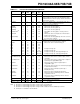
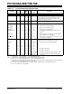
TABLE 4-1: SPECIAL FUNCTION REGISTER SUMMARY
Address Name Bit 7 Bit 6 Bit 5 Bit 4 Bit 3 Bit 2 Bit 1 Bit 0
Value on:
POR, BOR
Value on
all other
RESETS
(3)
Bank 0
00h INDF
(4)
Addressing this location uses contents of FSR to address data memory (not a physical register) 0000 0000 0000 0000
01h TMR0 Timer0 module’s register xxxx xxxx uuuu uuuu
02h PCL
(4)
Program Counter's (PC) Least Significant Byte 0000 0000 0000 0000
03h STATUS
(4)
IRP
(2)
RP1
(2)
RP0 TO PD ZDCC0001 1xxx 000q quuu
04h FSR
(4)
Indirect data memory address pointer xxxx xxxx uuuu uuuu
05h PORTA
— — PORTA Data Latch when written: PORTA pins when read --0x 0000 --0u 0000
06h PORTB PORTB Data Latch when written: PORTB pins when read xxxx xxxx uuuu uuuu
07h PORTC PORTC Data Latch when written: PORTC pins when read xxxx xxxx uuuu uuuu
08h PORTD
(5)
PORTD Data Latch when written: PORTD pins when read xxxx xxxx uuuu uuuu
09h PORTE
(5)
— — — — —RE2RE1RE0---- -xxx ---- -uuu
0Ah PCLATH
(1,4)
— — — Write Buffer for the upper 5 bits of the Program Counter ---0 0000 ---0 0000
0Bh INTCON
(4)
GIE PEIE T0IE INTE RBIE T0IF INTF RBIF 0000 000x 0000 000u
0Ch PIR1 PSPIF
(5)
ADIF
(6)
RCIF TXIF SSPIF CCP1IF TMR2IF TMR1IF 0000 0000 0000 0000
0Dh PIR2
— — — – — — —CCP2IF---- ---0 ---- ---0
0Eh TMR1L Holding register for the Least Significant Byte of the 16-bit TMR1 register xxxx xxxx uuuu uuuu
0Fh TMR1H Holding register for the Most Significant Byte of the 16-bit TMR1 register xxxx xxxx uuuu uuuu
10h T1CON
— — T1CKPS1 T1CKPS0 T1OSCEN T1SYNC TMR1CS TMR1ON --00 0000 --uu uuuu
11h TMR2 Timer2 module’s register 0000 0000 0000 0000
12h T2CON
— TOUTPS3 TOUTPS2 TOUTPS1 TOUTPS0 TMR2ON T2CKPS1 T2CKPS0 -000 0000 -000 0000
13h SSPBUF Synchronous Serial Port Receive Buffer/Transmit Register xxxx xxxx uuuu uuuu
14h SSPCON WCOL SSPOV SSPEN CKP SSPM3 SSPM2 SSPM1 SSPM0 0000 0000 0000 0000
15h CCPR1L Capture/Compare/PWM Register1 (LSB) xxxx xxxx uuuu uuuu
16h CCPR1H Capture/Compare/PWM Register1 (MSB) xxxx xxxx uuuu uuuu
17h CCP1CON
— — CCP1X CCP1Y CCP1M3 CCP1M2 CCP1M1 CCP1M0 --00 0000 --00 0000
18h RCSTA SPEN RX9 SREN CREN
— FERR OERR RX9D 0000 -00x 0000 -00x
19h TXREG USART Transmit Data register 0000 0000 0000 0000
1Ah RCREG USART Receive Data register 0000 0000 0000 0000
1Bh CCPR2L Capture/Compare/PWM Register2 (LSB) xxxx xxxx uuuu uuuu
1Ch CCPR2H Capture/Compare/PWM Register2 (MSB) xxxx xxxx uuuu uuuu
1Dh CCP2CON
— — CCP2X CCP2Y CCP2M3 CCP2M2 CCP2M1 CCP2M0 --00 0000 --00 0000
1Eh ADRES
(6)
A/D Result register xxxx xxxx uuuu uuuu
1Fh ADCON0
(6)
ADCS1 ADCS0 CHS2 CHS1 CHS0 GO/DONE —ADON0000 00-0 0000 00-0
Legend: x = unknown, u = unchanged, q = value depends on condition, - = unimplemented, read as '0'.
Shaded locations are unimplemented, read as ‘0’.
Note 1: The upper byte of the program counter is not directly accessible. PCLATH is a holding register for the PC<12:8>.
2: The IRP and RP1 bits are reserved; always maintain these bits clear.
3: Other (non power-up) RESETS include external RESET through MCLR
and Watchdog Timer Reset.
4: These registers can be addressed from either bank.
5: PORTD, PORTE and the parallel slave port are not implemented on the PIC16C63A/73B; always maintain these bits and
registers clear.
6: The A/D is not implemented on the PIC16C63A/65B; always maintain these bits and registers clear.