
Datasheet


1998-2013 Microchip Technology Inc. DS30605D-page 167
PIC16C63A/65B/73B/74B
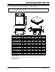
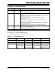
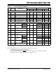
TABLE C-2: SPECIFICATION DIFFERENCES
Param
No.
Symbol Characteristic
PIC16C63/65A/73A/74A PIC16C63A/65B/73B/74B
Unit
Min Typ† Max Min Typ† Max
Core
D001
D001A
V
DD Supply Voltage 4.0
—
—
—
6.0
—
4.0
V
BOR
(1)
—
—
5.5
5.5
V
V
D005 BVDD Brown-out Reset Voltage 3.7 4.0 4.3 3.65 — 4.35 V
D150* V
OD Open-Drain High Voltage on
RA4
——14.0 - —8.5 V
A/D Converter
A20 V
REF Reference voltage 3.0 — VDD + 0.3 2.5 —VDD + 0.3 V
131 T
CNV Conversion time (Note 2)
(not including S/H time)
—9.5
(Note 3)
— 11
(Note 4)
— 11
(Note 4)
TAD
SSP in SPI mode
71 TscH SCK input high
time (Slave mode)
Continuous T
CY+20 — — 1.25TCY + 30 ——ns
71A Single Byte 40 ——ns
72 TscL SCK input low
time
(Slave mode)
Continuous T
CY+20 — — 1.25TCY + 30 ——ns
72A Single Byte 40 ——ns
73 TdiV2scH
TdiV2scL
Setup time of SDI data input to
SCK edge
50 — — 100 ——ns
73A
(Note 5)
T
B2B Last clock edge of Byte1 to the
1st clock edge of Byte2
—— —1.5TCY + 40 ——ns
74 TscH2diL
TscL2diL
Hold time of SDI data input to
SCK edge
50 — — 100 ——ns
75 TdoR SDO data output
rise time
PIC16CXX — 10 25 — 10 25 ns
PIC16LCXX — 20 45 ns
78 TscR SCK output rise
time (Master
mode)
PIC16CXX — 10 25 — 10 25 ns
PIC16LCXX — 20 45 ns
80 TscH2doV
TscL2doV
SDO data output
valid after SCK
edge
PIC16CXX — — 50 — — 50 ns
PIC16LCXX — — 100 ns
83 TscH2ssH
TscL 2ssH
SS
after SCK edge — — 50 1.5TCY + 40 ——ns
† Data in “Typ” column is at 5V, 25°C unless otherwise stated. These parameters are for design guidance only and are not
tested.
Note 1: When BOR is enabled, the device will operate until VDD drops below VBOR.
2: ADRES register may be read on the following T
CY cycle.
3: This is the time that the actual conversion requires.
4: This is the time from when the GO/DONE bit is set, to when the conversion result appears in ADRES.
5: Specification 73A is only required if specifications 71A and 72A are used.