
Datasheet


PIC16C63A/65B/73B/74B
DS30605D-page 138 1998-2013 Microchip Technology Inc.
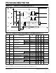
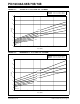
FIGURE 16-20: A/D CONVERSION TIMING
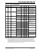
TABLE 16-17: A/D CONVERSION REQUIREMENTS
131
130
132
BSF ADCON0, GO
Q4
A/D CLK
A/D DATA
ADRES
ADIF
GO
SAMPLE
OLD_DATA
SAMPLING STOPPED
DONE
NEW_DATA
(T
OSC/2)
(1)
7 65432 10
Note 1: If the A/D clock source is selected as RC, a time of TCY is added before the A/D clock starts. This allows the SLEEP
instruction to be executed.
1 TCY
134
Param
No.
Sym Characteristic Min Typ† Max Units Conditions
130 T
AD A/D clock period PIC16CXX 1.6 — — sTOSC based, VREF 3.0 V
PIC16LCXX 2.0 — — sT
OSC based,
2.5V V
REF 5.5 V
PIC16CXX 2.0 4.0 6.0 s A/D RC mode
PIC16LCXX 3.0 6.0 9.0 s A/D RC mode
131 T
CNV Conversion time (not including S/H
time) (Note 1)
11 — 11 TAD
132 TACQ Acquisition time 5* — — s The minimum time is the
amplifier settling time. This
may be used if the “new”
input voltage has not
changed by more than 1 LSb
(i.e., 20.0mV @ 5.12V) from
the last sampled voltage (as
stated on C
HOLD).
134 T
GO Q4 to A/D clock start — TOSC/2 — — If the A/D clock source is
selected as RC, a time of T
CY
is added before the A/D clock
starts. This allows the SLEEP
instruction to be executed.
135 TSWC Switching from convert sample time 1.5 — — TAD
* These parameters are characterized but not tested.
† Data in “Typ” column is at 5V, 25C unless otherwise stated. These parameters are for design guidance only and
are not tested.
Note 1: ADRES register may be read on the following T
CY cycle.
2: See Section 12.1 for minimum conditions.