
Datasheet


1998-2013 Microchip Technology Inc. DS30605D-page 137
PIC16C63A/65B/73B/74B
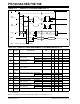
TABLE 16-16: A/D CONVERTER CHARACTERISTICS:
PIC16C73B/74B-04 (COMMERCIAL, INDUSTRIAL, EXTENDED)
PIC16C73B/74B-20 (COMMERCIAL, INDUSTRIAL, EXTENDED)
PIC16LC73B/74B-04 (COMMERCIAL, INDUSTRIAL)
Param
No.
Sym Characteristic Min Typ† Max Units Conditions
A01 N
R Resolution PIC16CXX — — 8 bits bit VREF = VDD = 5.12 V,
V
SS VAIN VREF
PIC16LCXX — — 8 bits bit
V
REF = VDD = 2.5 V
A02 EABS Total Absolute error — — < ± 1 LSb
V
REF = VDD = 5.12 V,
Vss V
AIN VREF
A03 EIL Integral linearity error — — < ± 1 LSb
V
REF = VDD = 5.12 V,
Vss V
AIN VREF
A04 EDL Differential linearity error — — < ± 1 LSb
V
REF = VDD = 5.12 V,
Vss V
AIN VREF
A05 EFS Full scale error — — < ± 1 LSb
V
REF = VDD = 5.12 V,
Vss V
AIN VREF
A06 EOFF Offset error — — < ± 1 LSb
V
REF = VDD = 5.12 V,
Vss V
AIN VREF
A10 — Monotonicity (Note 3) — guaranteed — —
Vss V
AIN VREF
A20 VREF Reference voltage 2.5V — VDD + 0.3 V
A25 V
AIN Analog input voltage VSS - 0.3 — VREF + 0.3 V
A30 Z
AIN Recommended impedance of
analog voltage source
——10.0k
A40 IAD A/D conversion
current (V
DD)
PIC16CXX — 180 — A
Average current
consumption when A/D
is on (Note 1)
PIC16LCXX — 90 — A
A50 I
REF VREF input current (Note 2) 10
—
—
—
1000
10
A
A
During V
AIN acquisition
Based on differential of
VHOLD to VAIN to charge
C
HOLD, see Section 12.1
During A/D Conversion
cycle
* These parameters are characterized but not tested.
† Data in “Typ” column is at 5 V, 25C unless otherwise stated. These parameters are for design guidance only and
are not tested.
Note 1: When A/D is off, it will not consume any current other than minor leakage current. The power-down current
spec includes any such leakage from the A/D module.
2: V
REF current is from the RA3 pin or the VDD pin, whichever is selected as a reference input.
3: The A/D conversion result never decreases with an increase in the input voltage and has no missing codes.