
Datasheet


1998-2013 Microchip Technology Inc. DS30605D-page 131
PIC16C63A/65B/73B/74B
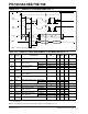
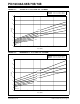
FIGURE 16-13: EXAMPLE SPI MASTER MODE TIMING (CKE = 1)
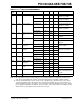
TABLE 16-9: EXAMPLE SPI MODE REQUIREMENTS (MASTER MODE, CKE = 1)
SS
SCK
(CKP = 0)
SCK
(CKP = 1)
SDO
SDI
81
71 72
74
75, 76
78
80
MSb
79
73
MSb IN
BIT6 - - - - - -1
LSb IN
BIT6 - - - -1
LSb
Note: Refer to Figure 16-4 for load conditions.
Param
No.
Symbol Characteristic Min Typ† Max Units Conditions
71 TscH SCK input high time
(Slave mode)
Continuous 1.25TCY + 30 — — ns
71A
Single Byte 40 — — ns (Note 1)
72
TscL SCK input low time
(Slave mode)
Continuous 1.25T
CY + 30 — — ns
72A
Single Byte 40 — — ns (Note 1)
73
TdiV2scH,
TdiV2scL
Setup time of SDI data input to SCK edge 100 — — ns
73A
T
B2B Last clock edge of Byte1 to the 1st clock
edge of Byte2
1.5TCY + 40 — — ns (Note 1)
74
TscH2 di L,
TscL2d iL
Hold time of SDI data input to SCK edge 100 — — ns
75
TdoR SDO data output rise
time
PIC16CXX — 10 25 ns
PIC16LCXX 20 45 ns
76
TdoF SDO data output fall time — 10 25 ns
78
TscR SCK output rise time
(Master mode)
PIC16CXX — 10 25 ns
PIC16LCXX 20 45 ns
79
TscF SCK output fall time (Master mode) — 10 25 ns
80
TscH2doV,
TscL2doV
SDO data output valid
after SCK edge
PIC16CXX — — 50 ns
PIC16LCXX — 100 ns
81
TdoV2scH,
TdoV2scL
SDO data output setup to SCK edge T
CY —— ns
† Data in “Typ” column is at 5 V, 25°C unless otherwise stated. These parameters are for design guidance only and
are not tested.
Note 1: Specification 73A is only required if specifications 71A and 72A are used.