
Datasheet


1998-2013 Microchip Technology Inc. DS30605D-page 13
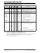
PIC16C63A/65B/73B/74B
PORTC is a bi-directional I/O port.
RC0/T1OSO/T1CKI 15 16 32 I/O ST RC0 can also be the Timer1 oscillator output or a
Timer1 clock input.
RC1/T1OSI/CCP2 16 18 35 I/O ST RC1 can also be the Timer1 oscillator input or Capture2
input/Compare2 output/PWM2 output.
RC2/CCP1 17 19 36 I/O ST RC2 can also be the Capture1 input/Compare1 output/
PWM1 output.
RC3/SCK/SCL 18 20 37 I/O ST RC3 can also be the synchronous serial clock input/
output for both SPI and I
2
C modes.
RC4/SDI/SDA 23 25 42 I/O ST RC4 can also be the SPI Data In (SPI mode) or
data I/O (I
2
C mode).
RC5/SDO 24 26 43 I/O ST RC5 can also be the SPI Data Out
(SPI mode).
RC6/TX/CK 25 27 44 I/O ST RC6 can also be the USART Asynchronous Transmit or
Synchronous Clock.
RC7/RX/DT 26 29 1 I/O ST RC7 can also be the USART Asynchronous Receive or
Synchronous Data.
PORTD is a bi-directional I/O port or parallel slave port
when interfacing to a microprocessor bus.
RD0/PSP0 19 21 38 I/O ST/TTL
(3)
RD1/PSP1 20 22 39 I/O ST/TTL
(3)
RD2/PSP2 21 23 40 I/O ST/TTL
(3)
RD3/PSP3 22 24 41 I/O ST/TTL
(3)
RD4/PSP4 27 30 2 I/O ST/TTL
(3)
RD5/PSP5 28 31 3 I/O ST/TTL
(3)
RD6/PSP6 29 32 4 I/O ST/TTL
(3)
RD7/PSP7 30 33 5 I/O ST/TTL
(3)
PORTE is a bi-directional I/O port.
RE0/RD
/AN5
(5)
8925I/OST/TTL
(3)
RE0 can also be read control for the parallel slave port,
or analog input 5
(5)
.
RE1/WR
/AN6
(5)
91026I/OST/TTL
(3)
RE1 can also be write control for the parallel slave port,
or analog input 6
(5)
.
RE2/CS
/AN7
(5)
10 11 27 I/O ST/TTL
(3)
RE2 can also be select control for the parallel slave
port, or analog input 7
(5)
.
V
SS 12,31 13,34 6,29 P — Ground reference for logic and I/O pins.
V
DD 11,32 12,35 7,28 P — Positive supply for logic and I/O pins.
NC — 1,17,28,
40
12,13,
33,34
— These pins are not internally connected. These pins should
be left unconnected.
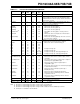
TABLE 3-2: PIC16C65B/74B PINOUT DESCRIPTION (CONTINUED)
Pin Name
DIP
Pin#
PLCC
Pin#
TQFP
MQFP
Pin#
I/O/P
Type
Buffer
Type
Description
Legend: I = input O = output I/O = input/output P = power
— = Not used TTL = TTL input ST = Schmitt Trigger input
Note 1: This buffer is a Schmitt Trigger input when configured as the external interrupt.
2: This buffer is a Schmitt Trigger input when used in Serial Programming mode.
3: This buffer is a Schmitt Trigger input when configured as general purpose I/O and a TTL input when used in the Parallel
Slave Port mode (for interfacing to a microprocessor bus).
4: This buffer is a Schmitt Trigger input when configured in RC oscillator mode and a CMOS input otherwise.
5: A/D is not available on the PIC16C65B.