
Datasheet


1998-2013 Microchip Technology Inc. DS30605D-page 121
PIC16C63A/65B/73B/74B
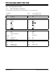
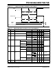
Capacitive Loading
Specs on
Output Pins
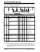
D100 C
OSC2 OSC2 pin – – 15 pF In XT, HS and LP modes when external
clock is used to drive OSC1
D101 CIO All I/O pins and OSC2
(in RC mode)
––50pF
D102 Cb SCL, SDA
(in I
2
C mode)
––400pF
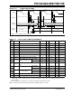
PIC16LC63A/65B/73B/74B-04
Standard Operating Conditions (unless otherwise stated)
Operating temperature 0°C TA +70°C for commercial
-40°C T
A +85°C for industrial
‡PIC16C63A/65B/73B/74B-04
‡PIC16C6A/65B/73B/74B-20
Standard Operating Conditions (unless otherwise stated)
Operating temperature 0°C T
A +70°C for commercial
-40°C T
A +85°C for industrial
-40°C T
A +125°C for extended
Param
No.
Sym Characteristic Min Typ† Max Units Conditions
* These parameters are characterized but not tested.
† Data in “Typ” column is at 5V, 25°C unless otherwise stated. These parameters are for design guidance only and
are not tested.
‡ When specification values of standard devices differ from those of extended voltage devices, they are shown in gray.
Note 1: This is the limit to which V
DD can be lowered without losing RAM data.
2: The supply current is mainly a function of the operating voltage and frequency. Other factors such as I/O pin
loading and switching rate, oscillator type, internal code execution pattern and temperature also have an impact
on the current consumption. The test conditions for all I
DD measurements in active operation mode are:
OSC1 = external square wave, from rail to rail; all I/O pins tri-stated, pulled to V
DD,
MCLR
= VDD; WDT enabled/disabled as specified.
3: The power-down current in SLEEP mode does not depend on the oscillator type. Power-down current is mea-
sured with the part in SLEEP mode, with all I/O pins in hi-impedance state and tied to V
DD and VSS.
4: For RC osc mode, current through R
EXT is not included. The current through the resistor can be estimated by
the formula Ir = V
DD/2REXT (mA) with REXT in kOhm.
5: Timer1 oscillator (when enabled) adds approximately 20 A to the specification. This value is from character-
ization and is for design guidance only. This is not tested.
6: The current is the additional current consumed when this peripheral is enabled. This current should be
added to the base I
DD or IPD measurement.
7: When BOR is enabled, the device will operate correctly until the V
BOR voltage trip point is reached.
8: In RC oscillator mode, the OSC1/CLKIN pin is a Schmitt Trigger input. It is not recommended that the PIC
device be driven with external clock in RC mode.
9: The leakage current on the MCLR
/VPP pin is strongly dependent on the applied voltage level. The specified lev-
els represent normal operating conditions. Higher leakage current may be measured at different input voltages.
10:Negative current is defined as current sourced by the pin.