
Datasheet


PIC16C63A/65B/73B/74B
DS30605D-page 10 1998-2013 Microchip Technology Inc.
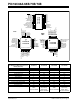
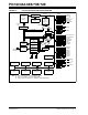
FIGURE 3-1: PIC16C63A/65B/73B/74B BLOCK DIAGRAM
EPROM
Program
Memory
13
Data Bus
8
14
Program
Bus
Instruction reg
Program Counter
8 Level Stack
(13-bit)
RAM
File
Registers
Direct Addr
7
RAM Addr
(1)
9
Addr MUX
Indirect
Addr
FSR reg
STATUS reg
MUX
ALU
W reg
Power-up
Timer
Oscillator
Start-up Timer
Power-on
Reset
Watchdog
Timer
Instruction
Decode &
Control
Timing
Generation
OSC1/CLKIN
OSC2/CLKOUT
MCLR
VDD, VSS
PORTA
PORTB
PORTC
PORTD
(3)
PORTE
(3)
RA4/T0CKI
RA5/SS
/AN4
(2)
RB0/INT
RB7:RB1
RC0/T1OSO/T1CKI
RC1/T1OSI/CCP2
RC2/CCP1
RC3/SCK/SCL
RC4/SDI/SDA
RC5/SDO
RC6/TX/CK
RC7/RX/DT
RD6/PSP6
RE0/RD
/AN5
(2,3)
RE1/WR/AN6
(2,3)
RE2/CS/AN7
(2,3)
8
8
Brown-out
Reset
Note 1: Higher order bits are from the STATUS register.
2: A/D is not available on the PIC16C63A/65B.
3: PSP and Ports D and E are not available on PIC16C63A/73B.
USART
CCP1 CCP2
Synchronous
A/D
(2)
Timer0 Timer1 Timer2
Serial Port
RA3/AN3/VREF
(2)
RA2/AN2
(2)
RA1/AN1
(2)
RA0/AN0
(2)
Parallel Slave Port
8
3
(3)
RD1/PSP1
RD2/PSP2
RD3/PSP3
RD4/PSP4
RD5/PSP5
RD0/PSP0
RD7/PSP7