
Datasheet


1997-2013 Microchip Technology Inc. DS30234E-page 279
PIC16C6X
Applicable Devices 61 62 62A R62 63 R63 64 64A R64 65 65A R65 66 67
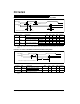
FIGURE 23-8: TYPICAL IPD vs. VDD BROWN-
OUT DETECT ENABLED (RC
MODE)
FIGURE 23-9: MAXIMUM I
PD vs. VDD
BROWN-OUT DETECT
ENABLED
(85C TO -40C, RC MODE)
The shaded region represents the built-in hysteresis of the
brown-out reset circuitry.
2.5 3.0 3.5 4.0 4.5 5.0 5.5 6.0
1400
1200
1000
800
600
400
200
0
V
DD(Volts)
IPD(A)
Device in
Brown-out
Device NOT in
Brown-out Reset
Reset
The shaded region represents the built-in hysteresis of the
brown-out reset circuitry.
2.5 3.0 3.5 4.0 4.5 5.0 5.5 6.0
1400
1200
1000
800
600
400
200
0
V
DD(Volts)
IPD(A)
4.3
1600
Device NOT in
Brown-out Reset
Device in
Brown-out
Reset
FIGURE 23-10: TYPICAL IPD vs. TIMER1
ENABLED (32 kHz, RC0/RC1 =
33 pF/33 pF, RC MODE)
FIGURE 23-11: MAXIMUM I
PD vs. TIMER1
ENABLED
(32 kHz, RC0/RC1 = 33 pF/33
pF, 85C TO -40C, RC MODE)
30
25
20
15
10
5
0
2.53.03.54.04.55.05.56.0
V
DD(Volts)
IPD(A)
30
25
20
15
10
5
0
2.5 3.0 3.5 4.0 4.5 5.0 5.5 6.0
V
DD(Volts)
IPD(A)
35
40
45
Data based on matrix samples. See first page of this section for details.