
Datasheet


1997-2013 Microchip Technology Inc. DS30234E-page 237
PIC16C6X
Applicable Devices 61 62 62A R62 63 R63 64 64A R64 65 65A R65 66 67
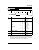
FIGURE 20-7: CAPTURE/COMPARE/PWM TIMINGS (CCP1 AND CCP2)
TABLE 20-6: CAPTURE/COMPARE/PWM REQUIREMENTS (CCP1 AND CCP2)
Parameter
No.
Sym Characteristic Min Typ† Max Units Conditions
50*
TccL CCP1 and CCP2
input low time
No Prescaler 0.5T
CY + 20 — — ns
With Prescaler PIC16C63/65A 10 — — ns
PIC16LC63/65A 20 — — ns
51* TccH
CCP1 and CCP2
input high time
No Prescaler 0.5T
CY + 20 — — ns
With Prescaler PIC16C63/65A 10 — — ns
PIC16LC63/65A 20 — — ns
52* TccP
CCP1 and CCP2 input period
3T
CY + 40
N
— — ns N = prescale value
(1,4, or 16)
53* TccR CCP1 and CCP2 output rise time PIC16C63/65A — 10 25 ns
PIC16LC63/65A — 25 45 ns
54* TccF CCP1 and CCP2 output fall time PIC16C63/65A — 10 25 ns
PIC16LC63/65A — 25 45 ns
* These parameters are characterized but not tested.
† Data in "Typ" column is at 5V, 25°C unless otherwise stated. These parameters are for design guidance only and are not
tested.
Note: Refer to Figure 20-1 for load conditions.
RC1/T1OSI/CCP2
and RC2/CCP1
(Capture Mode)
50 51
52
RC1/T1OSI/CCP2
and RC2/CCP1
53
54
PWM Mode)
(Compare or