
Datasheet


PIC16C6X
DS30234E-page 164 1997-2013 Microchip Technology Inc.
Applicable Devices 61 62 62A R62 63 R63 64 64A R64 65 65A R65 66 67
15.4 Timing Parameter Symbology
The timing parameter symbols have been created following one of the following formats:
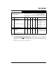
FIGURE 15-1: LOAD CONDITIONS FOR DEVICE TIMING SPECIFICATIONS
1. TppS2ppS
3. T
CC:ST (I
2
C specifications only)
2. TppS
4. Ts (I
2
C specifications only)
T
F Frequency T Time
Lowercase letters (pp) and their meanings:
pp
cc CCP1 osc OSC1
ck CLKOUT rd RD
cs CS rw RD or WR
di SDI sc SCK
do SDO ss SS
dt Data in t0 T0CKI
io I/O port t1 T1CKI
mc MCLR
wr WR
Uppercase letters and their meanings:
S
F Fall P Period
HHigh RRise
I Invalid (Hi-impedance) V Valid
L Low Z Hi-impedance
I
2
C only
AA output access High High
BUF Bus free Low Low
T
CC:ST (I
2
C specifications only)
CC
HD Hold SU Setup
ST
DAT DATA input hold STO STOP condition
STA START condition
VDD/2
C
L
RL
Pin Pin
V
SS
VSS
CL
RL = 464
C
L = 50 pF for all pins except OSC2/CLKOUT
15 pF for OSC2 output
Load condition 1
Load condition 2