
Datasheet


1997-2013 Microchip Technology Inc. DS30234E-page 103
PIC16C6X
11.5.2 MASTER MODE
Master mode of operation is supported in firmware
using interrupt generation on the detection of the
START and STOP conditions. The STOP (P) and
START (S) bits are cleared from a reset or when the
SSP module is disabled. The STOP (P) and START (S)
bits will toggle based on the START and STOP condi-
tions. Control of the I
2
C bus may be taken when the P
bit is set, or the bus is idle and both the S and P bits are
clear.
In master mode the SCL and SDA lines are manipu-
lated by clearing the corresponding TRISC<4:3> bit(s).
The output level is always low, irrespective of the
value(s) in PORTC<4:3>. So when transmitting data, a
'1' data bit must have the TRISC<4> bit set (input) and
a '0' data bit must have the TRISC<4> bit cleared (out-
put). The same scenario is true for the SCL line with the
TRISC<3> bit.
The following events will cause SSP Interrupt Flag bit,
SSPIF, to be set (SSP Interrupt if enabled):
• START condition
• STOP condition
• Data transfer byte transmitted/received
Master mode of operation can be done with either the
slave mode idle (SSPM3:SSPM0 = 1011) or with the
slave active. When both master and slave modes are
enabled, the software needs to differentiate the
source(s) of the interrupt.
11.5.3 MULTI-MASTER MODE
In multi-master mode, the interrupt generation on the
detection of the START and STOP conditions allows
the determination of when the bus is free. The STOP
(P) and START (S) bits are cleared from a reset or
when the SSP module is disabled. The STOP (P) and
START (S) bits will toggle based on the START and
STOP conditions. Control of the I
2
C bus may be taken
when bit P (SSPSTAT<4>) is set, or the bus is idle and
both the S and P bits clear. When the bus is busy,
enabling the SSP Interrupt will generate the interrupt
when the STOP condition occurs.
In multi-master operation, the SDA line must be moni-
tored to see if the signal level is the expected output
level. This check only needs to be done when a high
level is output. If a high level is expected and a low level
is present, the device needs to release the SDA and
SCL lines (set TRISC<4:3>). There are two stages
where this arbitration can be lost, these are:
• Address Transfer
• Data Transfer
When the slave logic is enabled, the slave continues to
receive. If arbitration was lost during the address trans-
fer stage, communication to the device may be in prog-
ress. If addressed an ACK
pulse will be generated. If
arbitration was lost during the data transfer stage, the
device will need to re-transfer the data at a later time.
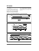
TABLE 11-5: REGISTERS ASSOCIATED WITH I
2
C OPERATION
Address Name Bit 7 Bit 6 Bit 5 Bit 4 Bit 3 Bit 2 Bit 1 Bit 0
Value on
POR,
BOR
Value on all
other resets
0Bh, 8Bh,
10Bh, 18Bh
INTCON GIE PEIE
T0IE INTE RBIE T0IF INTF RBIF
0000 000x 0000 000u
0Ch
PIR1
PSPIF
(1) (2)
RCIF TXIF SSPIF CCP1IF TMR2IF TMR1IF 0000 0000 0000 0000
8Ch
PIE1
PSPIE
(1) (2)
RCIE TXIE SSPIE CCP1IE TMR2IE TMR1IE 0000 0000 0000 0000
13h SSPBUF Synchronous Serial Port Receive Buffer/Transmit Register
xxxx xxxx uuuu uuuu
93h SSPADD Synchronous Serial Port (I
2
C mode) Address Register
0000 0000 0000 0000
14h SSPCON WCOL SSPOV SSPEN CKP SSPM3 SSPM2 SSPM1 SSPM0
0000 0000 0000 0000
94h SSPSTAT SMP
(3)
CKE
(3)
D/A PSR/WUA BF
0000 0000 0000 0000
87h TRISC
PORTC Data Direction register
1111 1111 1111 1111
Legend: x = unknown, u = unchanged, - = unimplemented locations read as '0'.
Shaded cells are not used by SSP module in SPI mode.
Note 1: PSPIF and PSPIE are reserved on the PIC16C66, always maintain these bits clear.
2: PIR1<6> and PIE1<6> are reserved, always maintain these bits clear.
3: The SMP and CKE bits are implemented on the PIC16C66/67 only. All other PIC16C6X devices have these two bits unim-
plemented, read as '0'.
Applicable Devices
61 62 62A R62 63 R63 64 64A R64 65 65A R65 66 67