
Datasheet


PIC16C6X
DS30234E-page 162 1997-2013 Microchip Technology Inc.
Applicable Devices 61 62 62A R62 63 R63 64 64A R64 65 65A R65 66 67
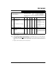
15.3 DC Characteristics: PIC16C61-04 (Commercial, Industrial, Extended)
PIC16C61-20 (Commercial, Industrial, Extended)
PIC16LC61-04 (Commercial, Industrial)
DC CHARACTERISTICS
Standard Operating Conditions (unless otherwise stated)
Operating temperature -40°C T
A +125°C for extended,
-40°C T
A +85°C for industrial and
0°C T
A +70°C for commercial
Operating voltage V
DD range as described in DC spec Section 15.1 and
Section 15.2.
Param
No.
Characteristic Sym Min Typ† Max Units Conditions
Input Low Voltage
I/O ports V
IL
D030
D030A
with TTL buffer Vss
V
SS
-
-
0.15VDD
0.8V
V
V
For entire V
DD range
4.5V V
DD 5.5V
D031 with Schmitt Trigger buffer Vss - 0.2V
DD V
D032 MCLR
, OSC1 (in RC mode) Vss - 0.2VDD V
D033 OSC1 (in XT, HS and LP) Vss - 0.3V
DD V Note1
Input High Voltage
I/O ports V
IH -
D040 with TTL buffer 2.0 - V
DD V4.5V VDD 5.5V
D040A 0.25V
DD
+ 0.8V
-V
DD V For entire VDD range
D041 with Schmitt Trigger buffer 0.85V
DD -VDD V For entire VDD range
D042 MCLR
0.85VDD -VDD V
D042A OSC1 (XT, HS and LP) 0.7V
DD -VDD V Note1
D043 OSC1 (in RC mode) 0.9V
DD -VDD V
D070 PORTB weak pull-up current I
PURB 50 250 † 400 AVDD = 5V, VPIN = VSS
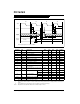
Input Leakage Current (Notes 2, 3)
D060 I/O ports I
IL --1 AVss VPIN VDD, Pin at hi-
impedance
D061 MCLR
, RA4/T0CKI - - 5 AVss VPIN VDD
D063 OSC1 - - 5 AVss VPIN VDD, XT, HS and
LP osc configuration
Output Low Voltage
D080 I/O ports V
OL --0.6VIOL = 8.5 mA, VDD = 4.5V,
-40C to +85C
D080A - - 0.6 V I
OL = 7.0 mA, VDD = 4.5V,
-40C to +125C
D083 OSC2/CLKOUT (RC osc config) - - 0.6 V I
OL = 1.6 mA, VDD = 4.5V,
-40C to +85C
D083A - - 0.6 V I
OL = 1.2 mA, VDD = 4.5V,
-40C to +125C
* The parameters are characterized but not tested.
† Data in “Typ” column is at 5V, 25C unless otherwise stated. These parameters are for design guidance only
and are not tested.
Note 1: In RC oscillator configuration, the OSC1/CLKIN pin is a Schmitt Trigger input. It is not recommended that the
PIC16C6X be driven with external clock in RC mode.
2: The leakage current on the MCLR
/VPP pin is strongly dependent on the applied voltage level. The specified
levels represent normal operating conditions. Higher leakage current may be measured at different input volt-
ages.
3: Negative current is defined as current sourced by the pin.