
Datasheet


PIC16C6X
DS30234E-page 140 1997-2013 Microchip Technology Inc.
13.7 Watchdog Timer (WDT)
The Watchdog Timer is a free running on-chip RC oscil-
lator which does not require any external components.
This RC oscillator is separate from the RC oscillator of
the OSC1/CLKIN pin. That means that the WDT will
run, even if the clock on the OSC1/CLKIN and OSC2/
CLKOUT pins of the device has been stopped, for
example, by execution of a SLEEP instruction. During
normal operation, a WDT time-out generates a device
reset. If the device is in SLEEP mode, a WDT time-out
causes the device to wake-up and continue with normal
operation (WDT Wake-up). The WDT can be perma-
nently disabled by clearing configuration bit WDTE
(Section 13.1).
13.7.1 WDT PERIOD
The WDT has a nominal time-out period of 18 ms, (with
no prescaler). The time-out periods vary with tempera-
ture, V
DD
and process variations from part to part (see
DC specs). If longer time-out periods are desired, a
prescaler with a division ratio of up to 1:128 can be
Applicable Devices
61 62 62A R62 63 R63 64 64A R64 65 65A R65 66 67
assigned to the WDT under software control by writing
to the OPTION register. Thus, time-out periods up to
2.3 seconds can be realized.
The CLRWDT and SLEEP instructions clear the WDT
and the postscaler, if assigned to the WDT, and prevent
it from timing out and generating a device RESET con-
dition.
The TO
bit in the STATUS register will be cleared upon
a WDT time-out.
13.7.2 WDT PROGRAMMING CONSIDERATIONS
It should also be taken in account that under worst case
conditions (V
DD = Min., Temperature = Max., max.
WDT prescaler) it may take several seconds before a
WDT time-out occurs.
Note: When a CLRWDT instruction is executed
and the prescaler is assigned to the WDT,
the prescaler count will be cleared, but the
prescaler assignment is not changed.
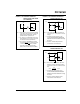
FIGURE 13-20: WATCHDOG TIMER BLOCK DIAGRAM
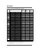
FIGURE 13-21: SUMMARY OF WATCHDOG TIMER REGISTERS
Address Name Bit 7 Bit 6 Bit 5 Bit 4 Bit 3 Bit 2 Bit 1 Bit 0
2007h Config. bits
(1)
BODEN
(1)
CP1 CP0
PWRTE
(1)
WDTE FOSC1 FOSC0
81h,181h OPTION
RBPU INTEDG T0CS T0SE PSA PS2 PS1 PS0
Legend: Shaded cells are not used by the Watchdog Timer.
Note 1: See Figure 13-1, Figure 13-2, and Figure 13-3 for details of these bits for the specific device.
From TMR0 Clock Source
(see Figure 7-6)
To TMR0 (Figure 7-6)
Watchdog
Timer
WDT
Enable bit
0
1
M
U
X
PSA
Postscaler
8- to -1 MUX
PS2:PS0
01
MUX
PSA
WDT
Time-out
8
Note: Bits T0CS, T0SE, PSA, PS2:PS0 are (OPTION<5:0>).