
Information

PIC16C63A/65B/73B/74B
DS80048C-page 2 2003 Microchip Technology Inc.
Clarifications/Corrections to the Data
Sheet:
In the Device Data Sheet (DS30605C), the following
clarifications and corrections should be noted:
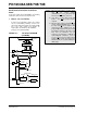
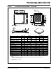
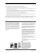
1. Module: SSP (SPI™ Mode)
In Section 10.2 (“SPI Mode”), Figure 10-1 and the
note box immediately following it have been
amended to better demonstrate the peripheral OE
line of the SSP module and describe its
relationship to the TRISC<5> bit of PORTC.
Changes are indicated in bold.
FIGURE 10-1: SSP BLOCK DIAGRAM
(SPI MODE)
Read Write
Internal
Data Bus
SSPSR reg
SSPM3:SSPM0
bit0
Shift
Clock
SS
Control
Enable
Edge
Select
Clock Select
TMR2 Output
T
CY
Prescaler
4, 16, 64
2
Edge
Select
2
4
TRISC<3>
2
SMP:CKE
RC4/SDI/SDA
RC5/SDO
RA5/SS
/AN4
RC3/SCK/SCL
SSPBUF reg
Peripheral OE
Note 1: When the SPI module is in Slave mode
with SS
pin control enabled
(SSPCON<3:0> = 0100), the SPI module
will reset if the SS pin is set to VDD.
2: If the SPI is used in Slave mode with
CKE = 1, then SS
pin control must be
enabled.
3: When the SPI is in Slave mode with SS pin
control enabled (SSPCON<3:0> = 0100 ),
the state of the SS
pin can affect the state
read back from the TRISC<5> bit. The
peripheral OE signal from the SSP module
into PORTC controls the state that is read
back from the TRISC<5> bit (see
Section 5.3 for information on PORTC). If
read-modify-write instructions, such as
BSF, are performed on the TRISC register
while the SS
pin is high, this will cause the
TRISC<5> bit to be set, thus disabling the
SDO output.