
Information

2001 Microchip Technology Inc. DS80094A-page 1
PIC16C63
The PIC16C63 (Rev. A) parts you have received con-
form functionally to the Device Data Sheet
(DS30234D), except for the anomalies described
below.
All the problems listed here will be addressed in future
revisions of the PIC16C63 silicon.
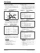
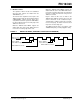
1. Module: CCP (Compare Mode)
The Compare mode may not operate as expected
when configuring the compare match to drive the
I/O pin low (CCPxM<3:0> = 1001).
When the CCP module is changed to compare
output low (CCPxM<3:0> = 1001) from any other
non-compare CCP mode, the I/O pin will immedi-
ately be driven low, regardless of the state of the
I/O data latch. The pin will remain low when the
compare match occurs (see Table 1).
However, when the CCP module is changed to
compare output high (CCPxM<3:0> = 1000) from
any other CCP mode, the I/O pin will immediately
be driven low, regardless of the state of the I/O
data latch. The pin will be driven high when the
compare match occurs.
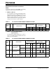
TABLE 1: COMPARE OUTPUT LOW
SWITCHING
Work around
To have the I/O pin high until the compare match
low occurs, force a compare match high to get the
I/O pin into the high state, then reconfigure the
compare match to force the I/O low when the com-
pare condition occurs.
2. Module: CCP (Compare Mode)
The special event trigger of the Compare mode
may not occur if both of the following conditions
exist:
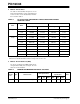
• An instruction, one cycle (T
CY) prior to a
Timer1/Compare register match has literal
data equal to the address of a CCP register
being used. Specific cases include:
• An instruction in the same cycle as a
Timer1/Compare register match has an
MSb of ‘0’.
The interrupt for the compare event will still be
generated, but no special event trigger will occur.
Work around
Use the Interrupt Service Routine instead of using
the special event trigger to reset Timer1 (and start
an A/D conversion, if applicable).
3. Module: SSP Module (I
2
C™ mode)
If the bus is active when the I
2
C mode is enabled,
and the next 8-bits of data on the bus match the
address of the device, then the SSP module will
generate an Acknowledge pulse.
Work around
Before enabling the I
2
C mode, ensure that the bus
is not active.
CCP Mode
CCPxM<3:0> =
I/O pin
State
Change CCP to
CCPxM<3:0> =
1001 1000
0xxx
HLL
LLL
1000
HH—
LL—
1001
H — L
L — L
101x
HLL
LLL
11xx
HLL
LLL
Unit Register Literal Data
CCP1
CCPR1L 15h
CCPR1H 16h
CCP1CON 17h
CCP2
CCPR2L 1Bh
CCPR2H 1Ch
CCP2C0N 1Dh
PIC16C63 Rev. A Silicon Errata Sheet