
Datasheet


2003 Microchip Technology Inc. DS30235J-page 103
PIC16C62X
12.8 Timing Parameter Symbology
The timing parameter symbols have been created with one of the following formats:
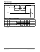
FIGURE 12-11: LOAD CONDITIONS
1. TppS2ppS
2. TppS
T
F Frequency T Time
Lowercase subscripts (pp) and their meanings:
pp
ck CLKOUT osc OSC1
io I/O port t0 T0CKI
mc MCLR
Uppercase letters and their meanings:
S
F Fall P Period
HHigh RRise
I Invalid (Hi-impedance) V Valid
L Low Z Hi-Impedance
VDD/2
CL
RL
Pin Pin
V
SS
VSS
CL
RL = 464Ω
C
L = 50 pF for all pins except OSC2
15 pF for OSC2 output
Load condition 1
Load condition 2