
Datasheet


PIC16C62X
DS30235J-page 102 2003 Microchip Technology Inc.
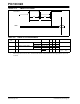
TABLE 12-1: COMPARATOR SPECIFICATIONS
Operating Conditions: VDD range as described in Table 12-1, -40°C<TA<+125°C. Current consumption is specified in
Table 12-1.
TABLE 12-2: VOLTAGE REFERENCE SPECIFICATIONS
Operating Conditions:VDD range as described in Table 12-1, -40°C<TA<+125°C. Current consumption is specified in
Table 12-1.
Characteristics Sym Min Typ Max Units Comments
Input offset voltage
± 5.0 ± 10 mV
Input common mode voltage
0V
DD - 1.5 V
CMRR
+55* δβ
Response Time
(1)
150*
400*
600*
ns
ns
PIC16C62X(A)
PIC16LC62X
Comparator mode change to
output valid
10* µs
* These parameters are characterized but not tested.
Note 1: Response time measured with one comparator input at (V
DD - 1.5)/2, while the other input transitions from
V
SS to VDD.
Characteristics Sym Min Typ Max Units Comments
Resolution
V
DD/24
V
DD/32
LSB
LSB
Low Range (V
RR=1)
High Range (V
RR=0)
Absolute Accuracy
+
1/4
+
1/2
LSB
LSB
Low Range (V
RR=1)
High Range (V
RR=0)
Unit Resistor Value (R)
2K* Ω
Figure 8-1
Settling Time
(1)
10* µs
* These parameters are characterized but not tested.
Note 1: Settling time measured while V
RR = 1 and VR<3:0> transitions from 0000 to 1111.