
Datasheet


2003 Microchip Technology Inc. DS30235J-page 101
PIC16C62X
12.6 DC Characteristics: PIC16C620A/C621A/C622A-40
(3)
(Commercial)
PIC16CR620A-40
(3)
(Commercial)
12.7 AC Characteristics: PIC16C620A/C621A/C622A-40
(2)
(Commercial)
PIC16CR620A-40
(2)
(Commercial)
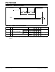
DC CHARACTERISTICS
Power Supply Pins
Standard Operating Conditions (unless otherwise stated)
Operating temperature 0°C ≤ TA ≤ +70°C for commercial
Characteristic Sym Min Typ
(1)
Max Units Conditions
Supply Voltage V
DD 4.5 — 5.5 V HS Option from 20 - 40 MHz
Supply Current
(2)
IDD —
—
5.5
7.7
11.5
16
mA
mA
FOSC = 40 MHz, VDD = 4.5V, HS mode
F
OSC = 40 MHz, VDD = 5.5V, HS mode
HS Oscillator Operating
Frequency
F
OSC 20 — 40 MHz OSC1 pin is externally driven,
OSC2 pin not connected
Input Low Voltage OSC1 V
IL VSS —0.2VDD V HS mode, OSC1 externally driven
Input High Voltage OSC1 V
IH 0.8VDD —VDD V HS mode, OSC1 externally driven
* These parameters are characterized but not tested.
Note 1: Data in the Typical (“Typ”) column is based on characterization results at 25°C. This data is for design guidance only and is
not tested.
2: The supply current is mainly a function of the operating voltage and frequency. Other factors such as bus loading, oscillator
type, bus rate, internal code execution pattern, and temperature also have an impact on the current consumption.
a) The test conditions for all I
DD measurements in Active Operation mode are:
OSC1 = external square wave, from rail-to-rail; all I/O pins tri-stated, pulled to V
SS,
T0CKI = V
DD, MCLR = VDD; WDT disabled, HS mode with OSC2 not connected.
3: For device operation between DC and 20 MHz. See Table 12-1 and Table 12-2.
AC CHARACTERISTICS
All Pins Except Power Supply Pins
Standard Operating Conditions (unless otherwise stated)
Operating temperature 0°C ≤ TA ≤ +70°C for commercial
Characteristic Sym Min Typ
(1)
Max Units Conditions
External CLKIN Frequency FOSC 20 — 40 MHz HS mode, OSC1 externally driven
External CLKIN Period TOSC 25 — 50 ns HS mode (40), OSC1 externally driven
Clock in (OSC1) Low or High Time TOSL, TOSH 6 — — ns HS mode, OSC1 externally driven
Clock in (OSC1) Rise or Fall Time TOSR, TOSF — — 6.5 ns HS mode, OSC1 externally driven
OSC1↑ (Q1 cycle) to Port out valid TOSH2IOV — — 100 ns —
OSC1↑ (Q2 cycle) to Port input
invalid (I/O in hold time)
TOSH2IOI 50 — — ns —
Note 1: Data in the Typical (“Typ”) column is at 5V, 25°C unless otherwise stated. These parameters are for design guidance only
and are not tested.
2: For device operation between DC and 20 MHz. See Table 12-1 and Table 12-2.