
Datasheet


PIC16C62X
DS30235J-page 100 2003 Microchip Technology Inc.
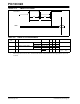
12.5 DC CHARACTERISTICS: PIC16C620A/C621A/C622A-40
(7)
(Commercial)
PIC16CR620A-40
(7)
(Commercial)
DC CHARACTERISTICS
Standard Operating Conditions (unless otherwise stated)
Operating temperature 0°C ≤ TA ≤ +70°C for commercial
Param
No.
Sym Characteristic Min Typ† Max Unit Conditions
VIL Input Low Voltage
I/O ports
D030 with TTL buffer VSS — 0.8V
0.15VDD
V VDD = 4.5V to 5.5V, otherwise
D031 with Schmitt Trigger input VSS 0.2VDD V
D032 MCLR, RA4/T0CKI, OSC1
(in RC mode)
VSS — 0.2VDD V (Note 1)
D033 OSC1 (in XT and HS)
OSC1 (in LP)
VSS
VSS
—
—
0.3VDD
0.6VDD - 1.0
V
V
VIH Input High Voltage
I/O ports
D040 with TTL buffer 2.0V
0.25 VDD + 0.8
— VDD
VDD
V VDD = 4.5V to 5.5V, otherwise
D041 with Schmitt Trigger input 0.8 VDD VDD
D042 MCLR RA4/T0CKI 0.8 VDD — VDD V
D043
D043A
OSC1 (XT, HS and LP)
OSC1 (in RC mode)
0.7 VDD
0.9 VDD
— VDD V
(Note 1)
D070 IPURB PORTB Weak Pull-up Current 50 200 400 µA VDD = 5.0V, VPIN = VSS
IIL Input Leakage Current
(2, 3)
I/O ports (except PORTA) ±1.0 µA VSS ≤ VPIN ≤ VDD, pin at hi-impedance
D060 PORTA — — ±0.5 µA Vss ≤ VPIN ≤ VDD, pin at hi-impedance
D061 RA4/T0CKI — — ±1.0 µA Vss ≤ VPIN ≤ VDD
D063 OSC1, MCLR — — ±5.0 µA Vss ≤ VPIN ≤ VDD, XT, HS and LP OSC con-
figuration
VOL Output Low Voltage
D080 I/O ports — — 0.6 V IOL = 8.5 mA, VDD = 4.5V, -40° to +85°C
— — 0.6 V IOL = 7.0 mA, VDD = 4.5V, +125°C
D083 OSC2/CLKOUT (RC only) — — 0.6 V IOL = 1.6 mA, VDD = 4.5V, -40° to +85°C
— — 0.6 V IOL = 1.2 mA, VDD = 4.5V, +125°C
VOH Output High Voltage
(3)
D090 I/O ports (except RA4) VDD-0.7 — — V IOH = -3.0 mA, VDD = 4.5V, -40° to +85°C
VDD-0.7 — — V IOH = -2.5 mA, VDD = 4.5V, +125°C
D092 OSC2/CLKOUT (RC only) VDD-0.7 — — V IOH = -1.3 mA, VDD = 4.5V, -40° to +85°C
VDD-0.7 — — V IOH = -1.0 mA, VDD = 4.5V, +125°C
*D150 VOD Open Drain High Voltage 8.5 V RA4 pin
Capacitive Loading Specs on
Output Pins
D100 COSC2 OSC2 pin 15 pF In XT, HS and LP modes when external
clock used to drive OSC1.
D101 CIO All I/O pins/OSC2 (in RC mode) 50 pF
* These parameters are characterized but not tested.
† Data in "Typ" column is at 5.0V, 25°C, unless otherwise stated. These parameters are for design guidance only and are
not tested.
Note 1: This is the limit to which V
DD can be lowered in SLEEP mode without losing RAM data.
2: The supply current is mainly a function of the operating voltage and frequency. Other factors such as I/O pin loading and switching rate,
oscillator type, internal code execution pattern, and temperature also have an impact on the current
consumption.
The test conditions for all I
DD measurements in Active Operation mode are:
OSC1 = external square wave, from rail-to-rail; all I/O pins tri-stated, pulled to V
DD, MCLR = VDD; WDT enabled/disabled as specified.
3: The power-down current in SLEEP mode does not depend on the oscillator type. Power-down current is measured with the part in SLEEP
mode, with all I/O pins in hi-impedance state and tied to V
DD or VSS.
4: For RC
OSC configuration, current through REXT is not included. The current through the resistor can be estimated by the formula Ir = VDD/
2R
EXT (mA) with REXT in kΩ.
5: The ∆ current is the additional current consumed when this peripheral is enabled. This current should be added to the base I
DD or IPD
measurement.
6: Commercial temperature range only.
7: See Section 12.1 and Section 12.3 for 16C62X and 16CR62X devices for operation between 20 MHz and 40 MHz for valid modified
characteristics.