
Information

PIC16C62X
DS80101D-page 14 2004 Microchip Technology Inc.
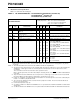
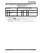
TABLE 2: DC CHARACTERISTICS: PIC16C620A/C621A/C622A-40
(4)
(Commercial)
PIC16CR620A-40
(4)
(Commercial)
PIC16CE62X-30
(5)
(Commercial)
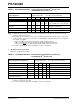
DC CHARACTERISTICS
Standard Operating Conditions (unless otherwise stated)
Operating temperature –40°C ≤ T
A ≤ +85°C for industrial and
0°C ≤ T
A ≤ +70°C for commercial and
–40°C ≤ T
A ≤ +125°C for extended
Parm
No.
Sym Characteristic Min Typ† Max Unit Conditions
V
IL Input Low Voltage
I/O ports
D030 with TTL buffer V
SS –0.8V
0.15V
DD
VVDD = 4.5V to 5.5V, otherwise
D031 with Schmitt Trigger input V
SS 0.2VDD V
D032 MCLR
, RA4/T0CKI, OSC1
(in RC mode)
VSS –0.2VDD V (Note 1)
D033 OSC1 (in XT and HS)
OSC1 (in LP)
V
SS
VSS
–
–
0.3VDD
0.6VDD - 1.0
V
V
V
IH Input High Voltage
I/O ports
D040 with TTL buffer 2.0V
.25V
DD + 0.8
–V
DD
VDD
VVDD = 4.5V to 5.5V, otherwise
D041 with Schmitt Trigger input 0.8V
DD VDD
D042 MCLR RA4/T0CKI 0.8VDD –VDD V
D043
D043A
OSC1 (XT, HS and LP)
OSC1 (in RC mode)
0.7V
DD
0.9VDD
–VDD V
(Note 1)
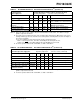
D070 I
PURB PORTB Weak Pull-up Current 50 200 400 µAVDD = 5.0V, VPIN = VSS
IIL Input Leakage Current
(Notes 2, 3)
I/O ports (except PORTA) ±1.0 µAV
SS ≤ VPIN ≤ VDD, pin at hi-impedance
D060 PORTA – – ±0.5 µA Vss ≤ V
PIN ≤ VDD, pin at hi-impedance
D061 RA4/T0CKI – – ±1.0 µA Vss ≤ V
PIN ≤ VDD
D063 OSC1, MCLR ––±5.0 µA Vss ≤ VPIN ≤ VDD, XT, HS and LP OSC
configuration
V
OL Output Low Voltage
D080 I/O ports – – 0.6 V I
OL=8.5 mA, VDD=4.5V, -40° to +85°C
––0.6VI
OL=7.0 mA, VDD=4.5V, +125°C
D083 OSC2/CLKOUT (RC only) – – 0.6 V I
OL=1.6 mA, VDD=4.5V, -40° to +85°C
––0.6VI
OL=1.2 mA, VDD=4.5V, +125°C
V
OH Output High Voltage (Note 3)
D090 I/O ports (except RA4) V
DD-0.7 – – V IOH=-3.0 mA, VDD=4.5V, -40° to +85°C
V
DD-0.7 – – V IOH=-2.5 mA, VDD=4.5V, +125°C
D092 OSC2/CLKOUT (RC only) V
DD-0.7 – – V IOH=-1.3 mA, VDD=4.5V, -40° to +85°C
V
DD-0.7 – – V IOH=-1.0 mA, VDD=4.5V, +125°C
*D150 V
OD Open Drain High Voltage 8.5 V RA4 pin
* These parameters are characterized but not tested.
† Data in “Typ” column is at 5.0V, 25°C unless otherwise stated. These parameters are for design guidance only and are not tested.
Note 1: In RC oscillator configuration, the OSC1 pin is a Schmitt Trigger input. It is not recommended that the PIC16CE62X be driven
with external clock in RC mode.
2: The leakage current on the MCLR
pin is strongly dependent on applied voltage level. The specified levels represent normal
operating conditions. Higher leakage current may be measured at different input voltages.
3: Negative current is defined as coming out of the pin.
4: See Table 3 and Table 4 for 16C62X and 16CR62X devices for operation between 20 MHz and 40 MHz for valid
modified characteristics.
5: See Table 5 and Table 6 for 16CE62X devices for operation between 20 MHz and 30 MHz for valid modified characteristics.