
Information


PIC16C62X
DS80101D-page 12 2004 Microchip Technology Inc.
2. Module: Electrical Specifications
Tables 1, 2, and 3 have been changed.
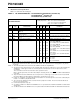
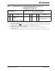
TABLE 1: DC CHARACTERISTICS: PIC16C620A/C621A/C622A-40
(7)
(Commercial)
PIC16CR620A-40
(7)
(Commercial)
PIC16CE62X-30
(8)
(Commercial)
DC CHARACTERISTICS
Standard Operating Conditions (unless otherwise stated)
Operating temperature –40°C ≤ T
A ≤ +85°C for industrial and
0°C ≤ T
A ≤ +70°C for commercial and
–40°C ≤ T
A ≤ +125°C for extended
Param
No.
Sym Characteristic Min Typ† Max Units Conditions
D001 V
DD Supply Voltage 3.0 – 5.5 V FOSC = DC to 20 MHz
D002 V
DR RAM Data Retention Voltage
(Note 1)
– 1.5* – V Device in SLEEP mode
D003 V
POR VDD start voltage to ensure
Power-on Reset
–VSS – V See section on Power-on Reset for details
D004 S
VDD VDD rise rate to ensure Power-on
Reset
0.05
*
– – V/ms See section on Power-on Reset for details
D005 V
BOR Brown-out Detect Voltage 3.65 4.0 4.35 V BOREN configuration bit is cleared
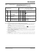
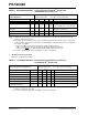
D010 I
DD Supply Current (Notes 2, 4) –
–
–
–
–
–
1.2
0.4
1.0
4.0
4.0
35
2.0
1.2
2.0
6.0
7.0
70
mA
mA
mA
mA
mA
µA
FOSC = 4 MHz, VDD = 5.5V, WDT disabled,
XT
OSC mode, (Note 4)*
F
OSC = 4 MHz, VDD = 3.0V, WDT disabled,
XT
OSC mode, (Note 4)
F
OSC = 10 MHz, VDD = 3.0V, WDT disabled,
HS
OSC mode, (Note 6)
F
OSC = 20 MHz, VDD = 4.5V, WDT disabled,
HS
OSC mode
F
OSC = 20 MHz, VDD = 5.5V, WDT disabled*,
HS
OSC mode
F
OSC = 32 kHz, VDD = 3.0V, WDT disabled,
LP
OSC mode
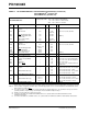
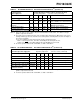
D020 I
PD Power Down Current (Note 3) –
–
–
–
–
–
–
–
2.2
5.0
9.0
15
µA
µA
µA
µA
VDD = 3.0V
V
DD = 4.5V*
V
DD = 5.5V
V
DD = 5.5V Extended
* These parameters are characterized but not tested.
† Data in "Typ" column is at 5.0V, 25°C, unless otherwise stated. These parameters are for design guidance only and are
not tested.
Note 1: This is the limit to which V
DD can be lowered in SLEEP mode without losing RAM data.
2: The supply current is mainly a function of the operating voltage and frequency. Other factors such as I/O pin loading and
switching rate, oscillator type, internal code execution pattern, and temperature also have an impact on the current
consumption.
The test conditions for all I
DD measurements in active operation mode are:
OSC1 = external square wave, from rail-to-rail; all I/O pins tri-stated, pulled to V
DD, MCLR = VDD; WDT enabled/disabled
as specified.
3: The power-down current in SLEEP mode does not depend on the oscillator type. Power-down current is measured with
the part in SLEEP mode, with all I/O pins in hi-impedance state and tied to V
DD or VSS.
4: For RC
OSC configuration, current through REXT is not included. The current through the resistor can be estimated by the
formula Ir = V
DD/2REXT (mA) with REXT in kΩ.
5: The ∆ current is the additional current consumed when this peripheral is enabled. This current should be added to the
base I
DD or IPD measurement.
6: Commercial temperature range only.
7: See Table 3 and Table 4 for 16C62X and 16CR62X devices for operation between 20 MHz and 40 MHz for valid modified
characteristics.
8: See Table 5 and Table 6 for 16CE62X devices for operation between 20 MHz and 30 MHz for valid modified characteristics.